Dislocation-free InSb quantum well structure on Si using novel buffer architecture

a quantum well and dislocation-free technology, applied in the field of buffer layer, can solve the problems of generating defects, iii-v material growth on silicon substrates, and iii-v material growth presents many challenges

Inactive Publication Date: 2009-08-11
INTEL CORP
View PDF7 Cites 43 Cited by
  • Summary
  • Abstract
  • Description
  • Claims
  • Application Information

AI Technical Summary

Problems solved by technology

Despite all these advantages, the growth of III-V materials upon silicon substrates presents many challenges.
When the lattice mismatch between the epitaxial layer and substrate exceeds a few percent, the strain induced by the mismatch becomes too great and defects are generated in the epitaxial layer when the epitaxial film relaxes.
Many defects, particularly threading dislocations and twins, tend to propagate into the “device layer” where the semiconductor device is fabricated.
The high defect density reduces the carrier mobility theoretically possible in bulk InSb, eliminating many of the technical advantages of “InSb-on-silicon” integration.
Similarly, a high defect density is also detrimental to photonic devices formed in or upon III-V semiconductor device layers on silicon substrates.

Method used


Image

  • Dislocation-free InSb quantum well structure on Si using novel buffer architecture
  • Dislocation-free InSb quantum well structure on Si using novel buffer architecture
  • Dislocation-free InSb quantum well structure on Si using novel buffer architecture

Examples


Embodiment Construction

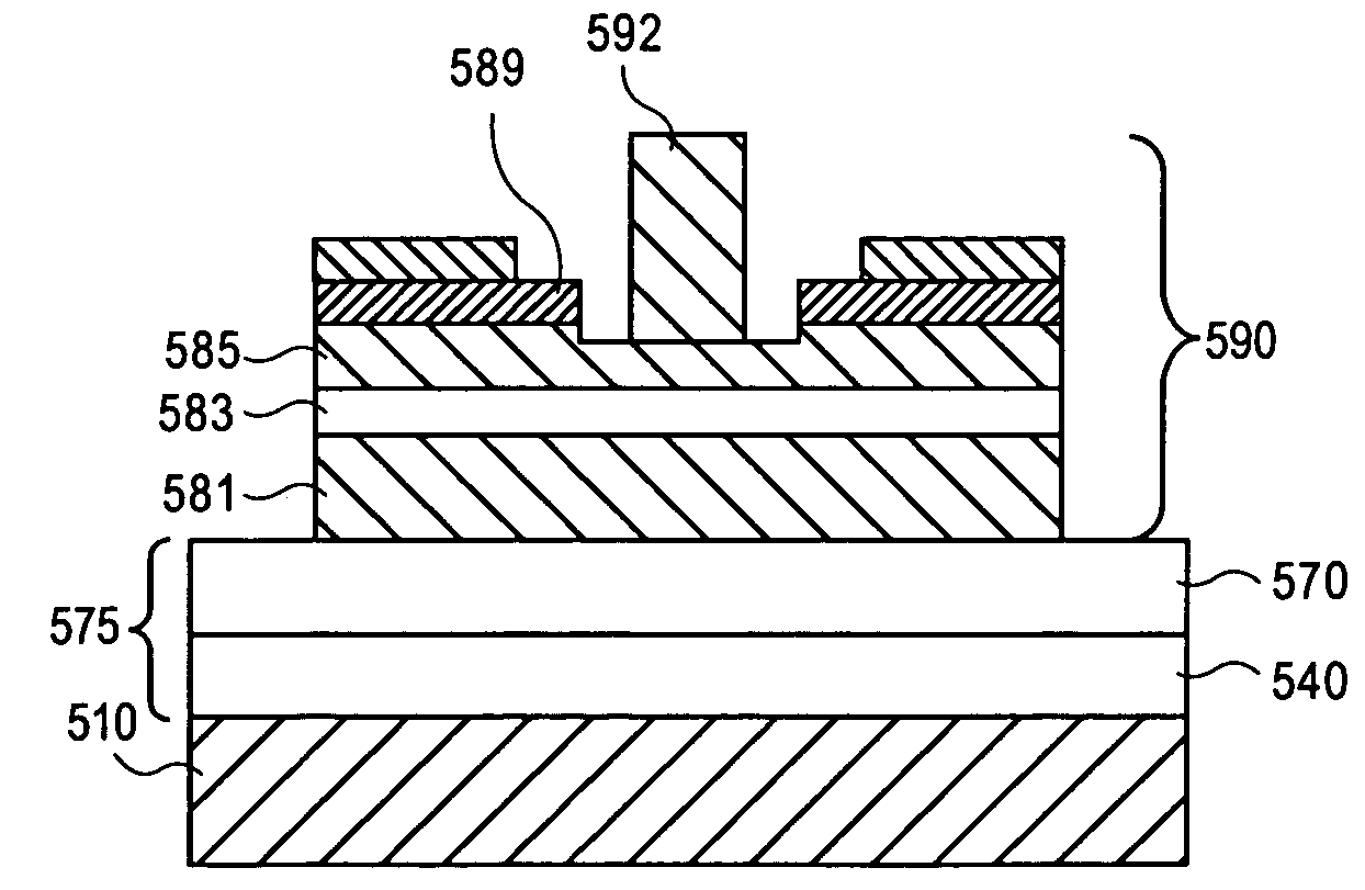
[0016]In various embodiments, a device grade III-V quantum well structure, formed on a silicon substrate using a composite buffer architecture, is described with reference to figures. However, certain embodiments may be practiced without one or more of these specific details, or in combination with other known methods and materials. In the following description, numerous specific details are set forth, such as specific materials, dimensions and processes, etc., in order to provide a thorough understanding of the present invention. In other instances, well-known semiconductor processes and manufacturing techniques have not been described in particular detail in order to not unnecessarily obscure the present invention. Reference throughout this specification to “an embodiment” means that a particular feature, structure, material, or characteristic described in connection with the embodiment is included in at least one embodiment of the invention. Thus, the appearances of the phrase “i...


PUM


Abstract

A device grade III-V quantum well structure formed on a silicon substrate using a composite buffer architecture and the method of manufacture is described. Embodiments of the present invention enable III-V InSb quantum well device layers with defect densities below 1×108 cm−2 to be formed on silicon substrates. In an embodiment of the present invention, an InSb quantum well layer is sandwiched between two larger band gap barrier layers. In an embodiment of the present invention, InSb quantum well layer is strained. In a specific embodiment, the two larger band gap barrier layers are graded.

Description

BACKGROUND OF THE INVENTION[0001]1. Field of the Invention[0002]The present invention relates to integrating III-V semiconductor devices upon silicon substrates. More particularly this invention relates to the buffer layer between a III-V semiconductor device and a silicon substrate.[0003]2. Discussion of Related Art[0004]A variety of electronic and optoelectronic devices can be enabled by developing thin film relaxed lattice constant III-V semiconductors on elemental silicon (Si) substrates. Surface layers capable of achieving the performance advantages of III-V materials may host a variety of high performance electronic devices such as CMOS and quantum well (QW) transistors fabricated from extreme high mobility materials such as, but not limited to, indium antimonide (InSb), indium gallium arsenide (InxGa1-xAs: x>0.53) and indium arsenide (InAs). Optical devices such as lasers, detectors and photovoltaics may also fabricated from various other direct band gap materials, such as...

Claims


Application Information

Patent Timeline
Patent Type & Authority Patents(United States)
IPC IPC(8): H01L29/06
CPCH01L21/02381H01L21/02466H01L21/02502H01L21/0251H01L21/02549H01L27/0605H01L29/045H01L29/205H01L29/267H01L29/66462H01L21/8252H01L31/0352
Inventor HUDAIT, MANTU K.SHAHEEN, MOHAMAD A.CHOW, LOREN A.TOLCHINSKY, PETER G.LOUBYCHEV, DMITRIFASTENAU, JOEL M.LIU, AMY W. K.
Owner INTEL CORP
Why Eureka
Try Eureka