Ferroelectric memory device and manufacturing method thereof

a technology of ferroelectric memory and manufacturing method, which is applied in the direction of semiconductor devices, capacitors, electrical apparatus, etc., can solve problems such as faulty electrical continuity, and achieve the effects of preventing oxidation of each plug due to the manufacturing process, preventing faulty electrical continuity of each plug, and efficient manufacturing

Inactive Publication Date: 2009-08-18
LAPIS SEMICON CO LTD
View PDF39 Cites 8 Cited by
  • Summary
  • Abstract
  • Description
  • Claims
  • Application Information

AI Technical Summary

Benefits of technology

[0038]According to the configuration of the ferroelectric memory device of the present invention, local wirings exist on their upper and lower sides respectively. The local wirings are sealed within areas partitioned by a plurality of hydrogen barrier films brought into closed bag forms as a whole by connecting their end edges to one another, i.e., they are encapsulated therein. Accordingly, there is no fear that each local wiring brings hydrogen inevitably existing within the device due to a manufacturing process like, for example, the formation of tungsten plugs, to a ferroelectric layer. That is, there is no fear that the ferroelectric layer is degraded. It is thus possible to provide a high-performance ferroelectric memory device free of degradation of an electrical characteristic and having a ferroelectric capacitor.
[0039]If such a configuration that the conductive hydrogen barrier films are provided even on top faces of all plugs is taken, then oxidation of each plug due to the manufacturing process can be prevented. That is, faulty electrical continuity of each plug can be prevented.
[0040]According to a method for manufacturing the ferroelectric memory device of the present invention, such a ferroelectric memory device as to have the above configuration can efficiently be manufactured in a simple process.
[0041]Even in the case of such a configuration that all the plugs are covered with the conductive hydrogen barrier films, an increase in the number of process steps is avoided and an efficient ferroelectric memory device can be manufactured.

Problems solved by technology

At this time, however, there is a case where when the surface of the plug is being exposed, the plug is oxidized, so that faulty electrical continuity occurs.

Method used


Image

  • Ferroelectric memory device and manufacturing method thereof
  • Ferroelectric memory device and manufacturing method thereof
  • Ferroelectric memory device and manufacturing method thereof

Examples


first preferred embodiment

(Configurational Example of Ferroelectric Memory Device)

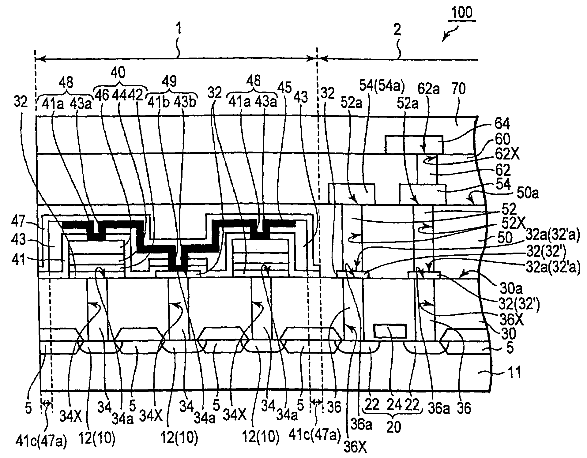
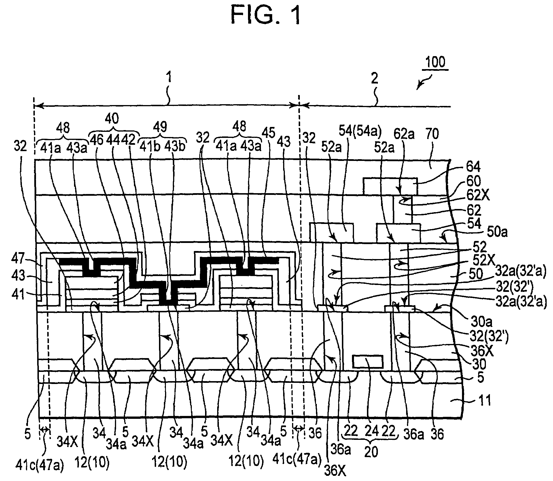
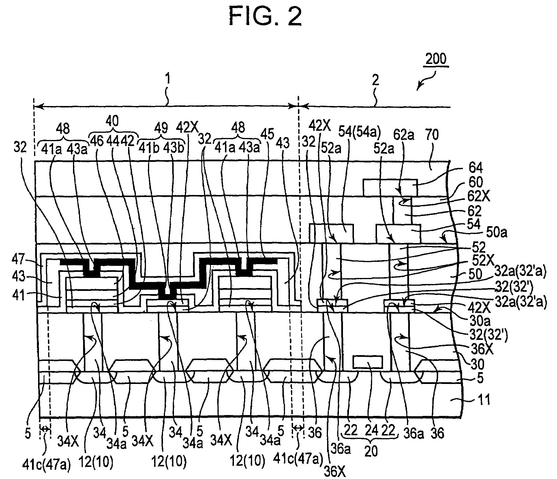
[0049]One configurational example of a ferroelectric memory device according to the present invention will be explained with reference to FIG. 1.

[0050]FIG. 1 is a typical view showing a partly-cutaway partial section of the ferroelectric memory device according to the present invention.

[0051]The ferroelectric memory device 100 according to the present invention is characterized by the constitution of an insulating hydrogen barrier film to be described later. As other constituent elements, arbitrary and suitable constituent elements of a conventional known ferroelectric memory device can be suitably selected and applied.

[0052]As shown in FIG. 1, the ferroelectric memory device 100 includes a semiconductor substrate 11. The semiconductor substrate 11 is compartmentalized by a memory cell array area 1 and a logic circuit area 2 adjacent to the memory cell array area 1.

[0053]The term “area” mentioned herein means a three-dimensiona...


PUM


Abstract

A ferroelectric memory device includes a semiconductor substrate, a first insulating film, a plurality of first and second plugs which extend through the first insulating film, conductive hydrogen barrier films, ferroelectric capacitor structural bodies, a first insulating hydrogen barrier film provided so as to cover the ferroelectric capacitor structural bodies, a second insulating film, local wirings extending on the second insulating film, a second insulating hydrogen barrier film which covers the local wirings, a third insulating film, third plugs which extend through the third insulating film so as to connect to their corresponding conductive hydrogen barrier films, and a first wiring layer extending on the third insulating film.

Description

BACKGROUND OF THE INVENTION[0001]The present invention relates to a ferroelectric memory device having memory cells each of which stores therein binarized data as a polarization state of a ferroelectric layer, and a manufacturing method thereof.[0002]An FeRAM (Ferroelectric Random Access Memory) has been known as a so-called ferroelectric memory.[0003]As one example of the ferroelectric memory, there has been known a configuration wherein an upper electrode of a capacitor including a ferroelectric layer and a W (tungsten)-plug connected to its corresponding elemental device are connected by a local wiring (refer to a non-patent document 1 (IEDM Digest of Technical papers. 1997, pp 613-616 (refer particularly to FIG. 1)).[0004]There has also been known a configuration wherein a lower electrode of a capacitor including a ferroelectric layer and a W (tungsten)-plug connected to its corresponding elemental device are directly connected (refer to a non-patent document 2 (IEDM Digest of T...

Claims


Application Information

Patent Timeline
Patent Type & Authority Patents(United States)
IPC IPC(8): H01L21/8242
CPCH01L21/76834H01L21/7687H01L21/76895H01L27/105H01L28/75H01L27/11507H01L27/11509H01L28/57H01L28/65H01L27/11502H10B53/40H10B53/30H10B53/00H10B12/00
Inventor HAYASHI, TAKAHISA
Owner LAPIS SEMICON CO LTD
Why Eureka
Try Eureka