Method and compositions for direct copper plating and filing to form interconnects in the fabrication of semiconductor devices

a technology of direct copper plating and semiconductor devices, applied in the direction of tobacco, transportation and packaging, packaging goods types, etc., can solve the problems of insufficient step coverage of pvd techniques, difficulty in filling copper pipes, and inherently directional pvd techniques, etc., to achieve low resistance, strong adhesion, and low resistance

Active Publication Date: 2009-08-25
ALCHIMER SA
View PDF12 Cites 13 Cited by
  • Summary
  • Abstract
  • Description
  • Claims
  • Application Information

AI Technical Summary

Benefits of technology

[0024]In accordance with the present invention, it has been discovered that a single electrolytic copper bath may be used to electroplate copper directly onto a copper diffusion barrier material which can be pre-treated or not, with the resulting copper film completely filling, without any defects such as “seam”, the trenches, vias and other features previously covered with the barrier material. It has been found surprisingly that the copper thus deposited exhibits low resistivity after annealing and strong adhesion to the underlying barrier. Low resistivity is particularly advantageous to ensure low signal propagation delays and good adhesion is particularly advantageous to ensure good electromigration resistance. It has also been found surprisingly that said electrolytic copper bath allows gap filling to be reached after a relatively short deposition time which is compatible with industrial process requirements.

Problems solved by technology

As a result, the aspect ratio of the lines and vias, defined as their height-to-width ratio, tends to increase, making it difficult to fill them with copper.
These increasingly shrinking dimensions are a serious problem when physical deposition processes such as PVD have to be used as it is the case for the seed layer deposition in the damascene sequence.
The PVD techniques are inherently directional and thus do not have adequate step coverage to meet these requirements for small features and / or for high aspect ratios.
This constriction of the feature width prior to copper electroplating makes achieving complete gapfill very challenging.
This thickness requirement combined with the poor conformality of PVD processes result in discontinuities in the seed layer which appear on the feature sidewalls leading to defective and incomplete copper gap filling.
Alternate deposition techniques such as chemical vapor deposition (CVD) or atomic layer deposition (ALD) can be used to deposit a copper seed layer [see U.S. Pat. Nos. 6,887,522 and 6,849,122] but these processes still suffer from some type of overhang effect and they are prone to produce poor adhesion of copper to the underlying barrier layer due to the use of fluorine-containing precursors, thus compromising device yield.
These CVD and ALD processes cannot be used for filling features as their deposition rate is very low, making them incompatible with the high productivity environment of semiconductor device manufacturing.
However, an extra activation step is often required and adhesion is also a problem.
This approach has the disadvantage of introducing a new material and requires significant rework of some of the processes of the damascene sequence.
As feature dimensions decrease, the use of seed layers will more significantly contribute to increase the effective aspect ratio and make gap filling by copper electroplating even more difficult, if merely possible.
An electrolytic copper bath capable of forming a seed layer of copper is normally not usable for gap filling since it generally leads to an inappropriate coating with the formation of a filling defect known as a “seam” (a central notch in the via, appearing when the filling gradient occurs predominantly from the lateral walls of the via).
Such a seam may cause a structural weakness due to a locally low copper density.
Alternatively, traditional electroplating baths, such as those which are being used to fill up trenches after a copper seed step, cannot afford uniform coverage starting directly on the barrier material, due to ohmic drop effects: existing copper electroplating bath are indeed designed to perform bottom-up copper growth on a conductive surface.
Last, filling trenches in a single step constitutes a difficult challenge as one is actually seeking the process to start as a conformal deposition, in order to avoid overhang and / or discontinuities, and then to continue in a non-conformal or bottom-up growth to secure complete seamless filling.
A gap fill capable single step electroplating performed directly on the diffusion barrier material would thus alleviate the above issues and constitute a solution not necessarily straightforward to the skilled person.

Method used


Image

  • Method and compositions for direct copper plating and filing to form interconnects in the fabrication of semiconductor devices
  • Method and compositions for direct copper plating and filing to form interconnects in the fabrication of semiconductor devices

Examples


example 1

[0092]The substrate used in this example consisted of a silicon workpiece, coated with a 400 nm layer of silicon dioxide deposited by plasma-enhanced chemical vapor deposition (PECVD). The silicon dioxide layer was coated with a layer of tantalum nitride (TaN) having a thickness of 10 nm deposited by PVD on top of which a layer of tantalum (Ta) having a thickness of 15 nm was also deposited by PVD.

[0093]This TaN / Ta stack is a copper diffusion barrier such as those used in damascene structures. The sheet resistance of this barrier stack was 21 ohm / square.

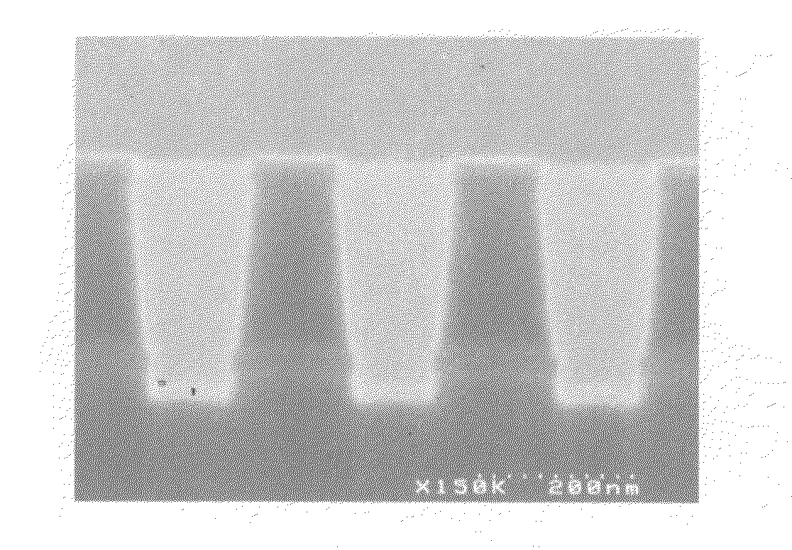
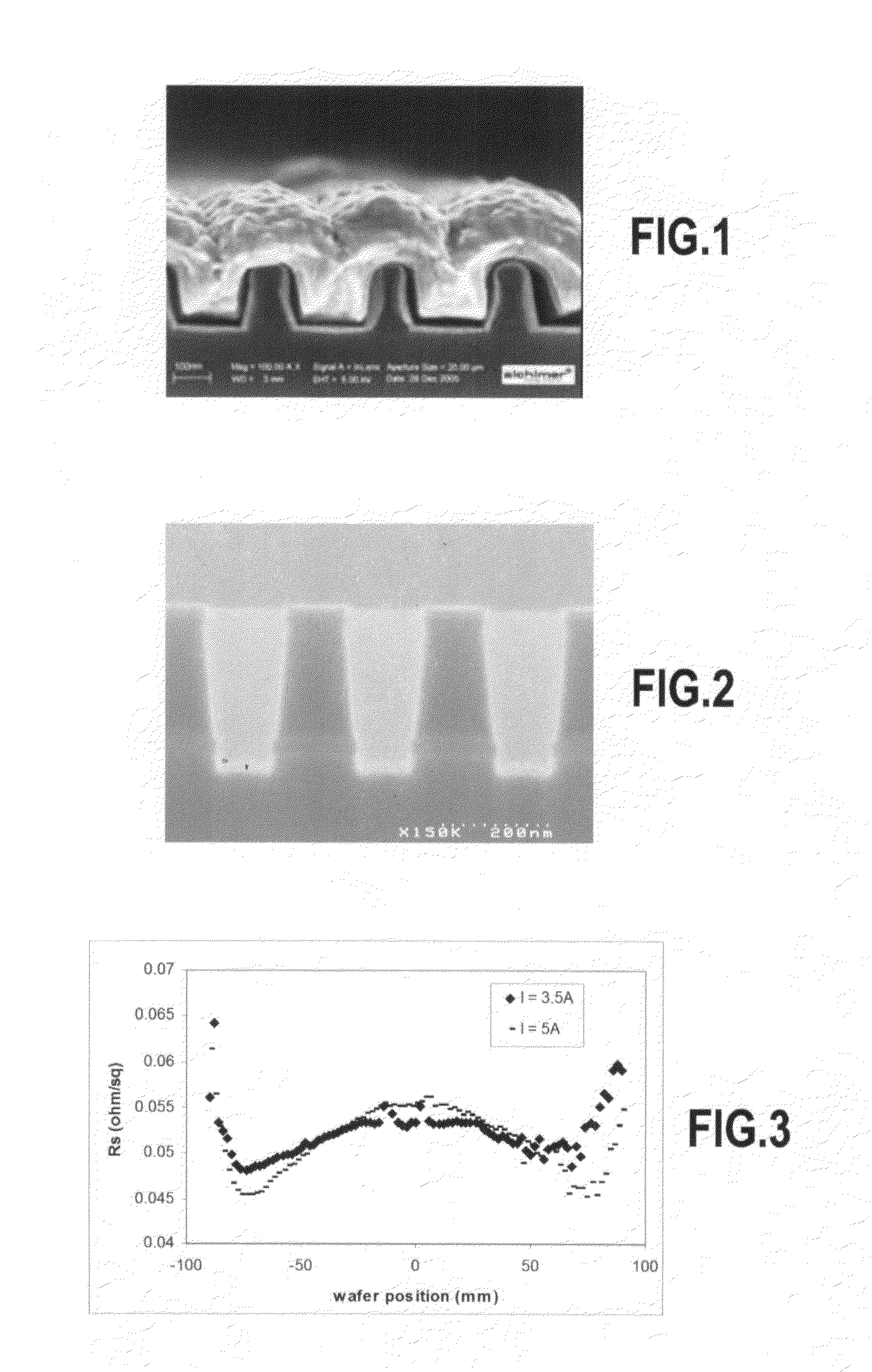
[0094]A blanket substrate was used for sheet resistance (Rs) measurement by 4-point probe. Adhesion on a blanket substrate was measured by a variable force stud-pull test. A trench-patterned substrate (trench width 200 nm / spacing 100 nm) having the same underlayers as the blanket substrate was used for gap-filling evaluation. Gap fill was observed by scanning electron microscope (SEM) cross-sectional imaging.

[0095]These substrates we...

example 2

[0106]The substrate used in this example consisted of a silicon workpiece, coated with a 400 nm layer of silicon dioxide deposited by plasma-enhanced chemical vapor deposition (PECVD). The silicon dioxide layer was coated with a layer of ruthenium (Ru) having a thickness of 30 nm deposited by PVD. The sheet resistance of this ruthenium layer was 8.5 Ohm / square.

[0107]A blanket substrate was used for sheet resistance (Rs) measurement by 4-point probe. Adhesion on a blanket substrate was measured by a variable force stud-pull test.

[0108]These substrates were used without any pre-treatment.

[0109]The electrolytic copper bath of the invention in this particular example was an aqueous solution containing CuSO4,(H2O)5 with a concentration of 65 mM, and ethylenediamine with a concentration of 160 mM. The pH of this solution was 11.

Equipment

[0110]The cell used for the electrolytic deposit was a glass cell made up of two parts: the cell intended to contain the solution for electrodeposition an...

example 3

[0118]The substrate used in this example consisted of a silicon wafer of diameter 200 mm, coated with a 400 nm layer of silicon dioxide deposited by plasma-enhanced chemical vapor deposition (PECVD). The silicon dioxide layer was coated with a layer of tantalum nitride (TaN) having a thickness of 15 nm deposited by PVD on top of which a layer of tantalum (Ta) having a thickness of 10 nm was also deposited by PVD.

[0119]This TaN / Ta stack is a copper diffusion barrier such as those used in damascene structures. The sheet resistance of this barrier stack was 45 ohm / square.

[0120]A blanket substrate was used for sheet resistance (Rs) measurement by 4-point probe. Adhesion on a blanket substrate was measured by a scotch tape test. A trench-patterned substrate (trench width 200 nm / spacing 100 nm) having the same underlayers as the blanket substrate was used for gap-filling evaluation. Gap fill was observed by focused ion beam (FIB) and SEM cross-sectional imaging.

[0121]These substrates were...


PUM

PropertyMeasurementUnit
molar ratioaaaaaaaaaa

Abstract

The object of the present invention is a method and compositions for direct copper plating and filling to form interconnects in the fabrication of semiconductor devices.According to the invention, this method comprises:providing an electrolytic copper bath containing, in solution in a solvent, a source of copper ions with a concentration of between 45 and 200 mM, preferably of between 45 and 100 mM and at least one copper complexing agent which is an aliphatic polyamine having 2 to 4 amine functions with a concentration of between 30 and 200 mM, preferably of between 60 and 200 mM; the copper / complexing agent(s) molar ratio being of between 0.2 and 2, preferably between 0.3 and 1.5;bringing said copper diffusion barrier layer of said substrate into contact with said electrolytic copper bath,applying an electrical bias to the substrate for a duration adjusted according to the thickness of copper to be electroplated,removing the substrate from said electrolytic copper bath.

Description

[0001]The present application claims benefit of U.S. provisional application 60 / 774,675 filed Feb. 21, 2006.[0002]The present invention generally concerns a method and compositions for direct copper plating and filling to form interconnects in the fabrication of semiconductor devices.BACKGROUND OF THE INVENTION [0003]Copper metallization has become widely adopted to form the multilevel interconnects required in today's ultra large scale integration (ULSI) semiconductor devices, due to its lower resistivity compared to aluminum and its improved electromigration resistance.[0004]Multilevel interconnects consist in a network of copper lines (also called trenches) that are used to distribute various signals as well as power and ground to different areas of an integrated circuit. In order to be more real estate-efficient, these lines are stacked in several levels separated by a dielectric material and levels are connected to each other through vertical apertures called vias.[0005]Lines a...

Claims


Application Information

Patent Timeline
Patent Type & Authority Patents(United States)
IPC IPC(8): H01L21/44
CPCC25D3/38H01L21/76877H01L21/2885C25D5/54C25D5/18C25D5/627C25D5/611C25D7/123
Inventor GONZALEZ, JOSEMONCHOIX, HERVE
Owner ALCHIMER SA
Why Eureka
Try Eureka