MIS-type field-effect transistor

a field-effect transistor and field-effect transistor technology, applied in transistors, knitting, weaving, etc., can solve the problems of low electron-hole mobility of the si and decrease the switching speed of the misfet, and achieve the effects of preventing the formation of doping-induced dislocations, small channel length, and low power consumption

Active Publication Date: 2009-08-25
GK BRIDGE 1
View PDF25 Cites 0 Cited by
  • Summary
  • Abstract
  • Description
  • Claims
  • Application Information

AI Technical Summary

Benefits of technology

[0023]Since the MISFET of the present invention is designed so that the film thickness of the strained active semiconductor layer is no more than twice the depth Tp of maximum concentration of the impurity introduced for forming the source / drain region, or the film thickness of the built-up region formed on the strained active semiconductor layer is no less than three times the depth Tp, it is possible to prevent the formation of doping-induced dislocations in the strained active semiconductor layer. There is therefore no growth of U-shaped dislocations around these nuclei in the strained active semiconductor layer. As a result, a strained-channel MISFET can be obtained that has low power consumption, small channel length, and zero occurrence of abnormal off-leakage currents even when the gate in the MISFET is short.

Problems solved by technology

However, Si suffers from low electron-hole mobility compared to other semiconductors.
Low mobility causes the channel resistance of a MISFET to increase, which leads to decreased switching speed in the MISFET.

Method used


Image

  • MIS-type field-effect transistor
  • MIS-type field-effect transistor
  • MIS-type field-effect transistor

Examples


first embodiment

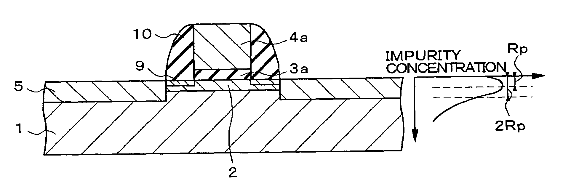
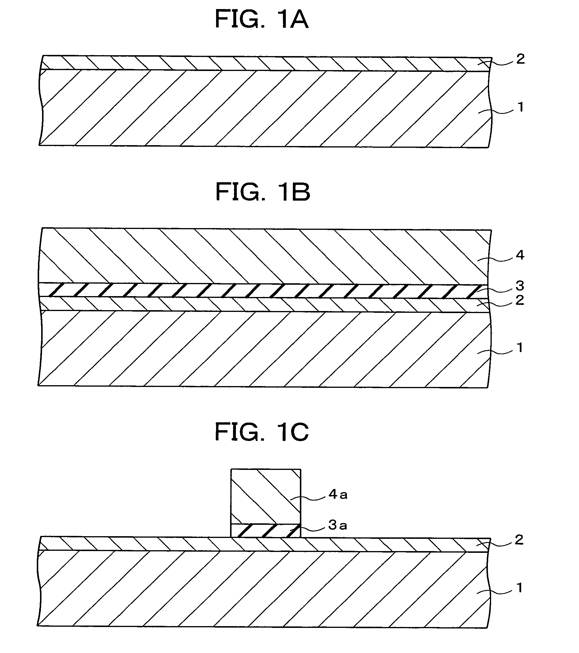
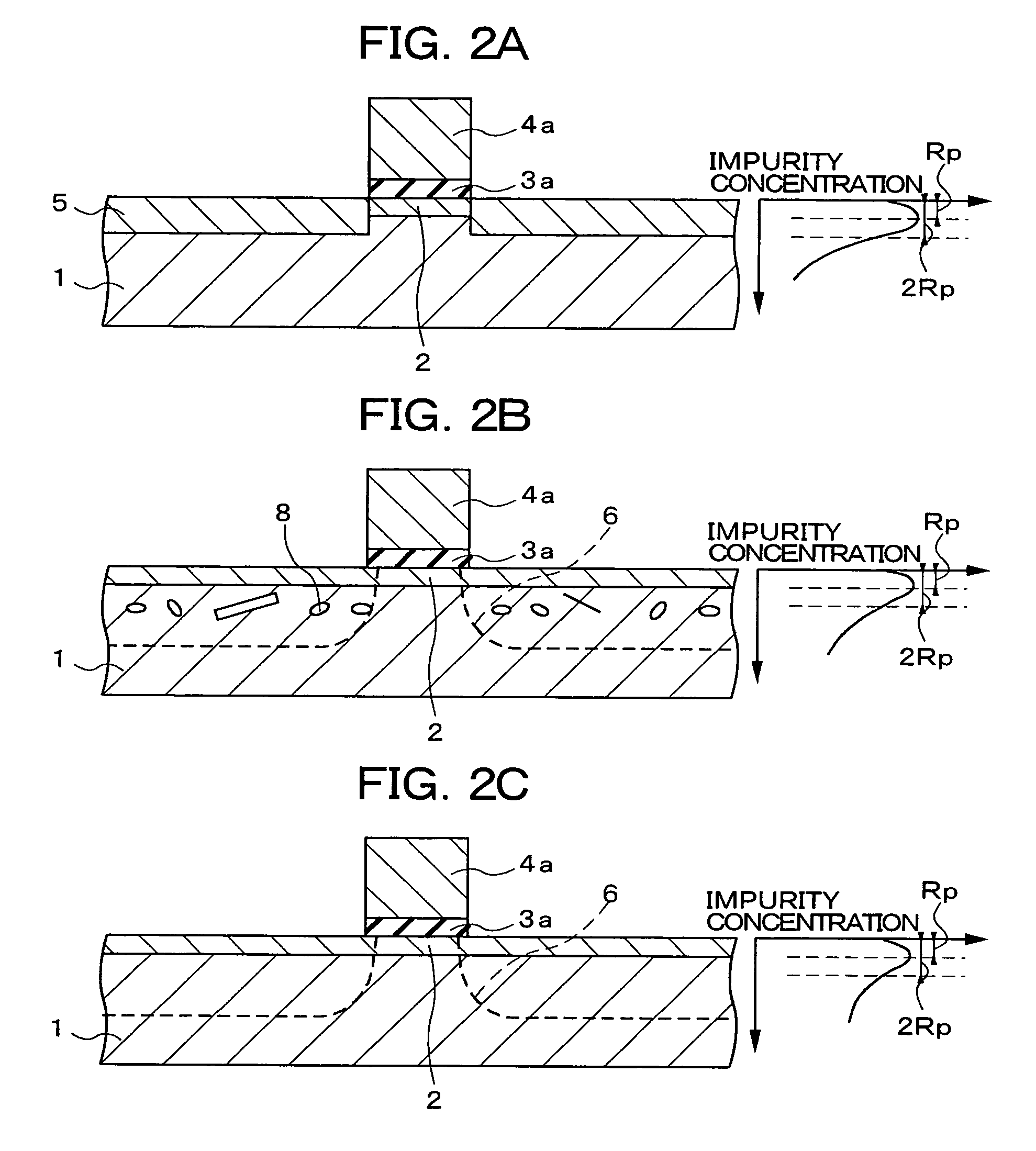
[0109]FIGS. 1A through 1C and FIGS. 2A through 2C are sectional views showing the sequence of steps in the method for manufacturing a MISFET according to a first embodiment of the present invention. First, a strained Si layer 2 is epitaxially grown on the base SiGe layer 1 (FIG. 1A). The film thickness of this strained Si layer 2 is set to 2Tp or less, where Tp is the depth at which the impurity concentration of the source / drain of the final MISFET is at maximum. A gate insulating film 3 and a gate electrode film 4 are then grown thereon (FIG. 1B), after which patterning is performed, and a gate insulating film 3a and a gate electrode 4a having a length of 0.4 μm or less are formed (FIG. 1C). An impurity in the amount of 1×1015 cm−2 or higher is then ion-implanted into the strained Si layer 2 and the base SiGe layer 1 using the gate electrode 4a as a mask. An impurity is thus introduced at high concentration into the region in which the source / drain is to be formed, and an amorphous...

second embodiment

[0111]FIGS. 3A through 3C, FIGS. 4A through 4C, and FIGS. 5A and 5B are sectional views showing the sequence of steps in the method for manufacturing a MISFET according to a second embodiment of the present invention. First, a strained Si layer 2 is epitaxially grown on the base SiGe layer 1. The film thickness of this strained Si layer 2 is set to 2Tp or less, where Tp is the depth at which the impurity concentration of the source / drain of the final MISFET is at maximum (FIG. 3A). A gate insulating film 3 and a gate electrode film 4 are then grown thereon (FIG. 3B), after which patterning is performed, and a gate insulating film 3a and a gate electrode 4a having a length of 0.4 μm or less are formed (FIG. 3C).

[0112]An impurity for forming a source / drain extension region is then ion-implanted into the strained Si layer 2 using the gate electrode 4a as a mask, and an impurity-implanted region 9 is formed (FIG. 4A). In this instance, the implantation energy and dose are reduced compar...

third embodiment

[0115]FIGS. 7A through 7C, FIGS. 8A through 8C, and FIGS. 9A through 9C are sectional views showing the sequence of steps in the method for manufacturing a MISFET according to a third embodiment of the present invention. First, a strained Si layer 2 is epitaxially grown on the base SiGe layer 1 (FIG. 7A). The film thickness of this strained Si layer 2 may be 2Tp or greater, where Tp is the depth at which the impurity concentration of the source / drain of the final MISFET is at maximum. A gate insulating film 3 and a gate electrode film 4 are then grown thereon (FIG. 7B), after which patterning is performed, and a gate insulating film 3a and a gate electrode 4a having a length of 0.4 μm or less are formed (FIG. 7C).

[0116]An impurity for forming a source / drain extension region is then ion-implanted into the strained Si layer 2 using the gate electrode 4a as a mask, and an impurity-implanted region 9 is formed (FIG. 8A). In this instance, the implantation energy and dose are reduced com...


PUM

PropertyMeasurementUnit
thicknessaaaaaaaaaa
gate lengthaaaaaaaaaa

Abstract

A strained Si layer 2 is epitaxially grown on a base SiGe layer 1, and a gate insulating film 3a and a gate electrode 4a are formed. An impurity is then ion-implanted (FIG. 2A) into the base SiGe layer 1 and the strained Si layer 2 using the gate electrode 4a as a mask, heat treatment is performed for activation, and a source / drain region 6 is formed (FIGS. 2B and 2C). In this instance, the film thickness of the strained Si layer 2 is set to 2Tp, where Tp (=Rp) is the depth having the maximum concentration of the impurity in the source / drain region 6 of the finished MISFET.

Description

TECHNICAL FIELD[0001]The present invention relates to an MIS-type field-effect transistor, and particularly relates to an MIS-type field-effect transistor formed from a semiconductor having a strained channel.BACKGROUND ART[0002]MIS-type field-effect transistors (hereinafter abbreviated as MISFET) are commonly formed on group IV semiconductor substrates. The term “group IV semiconductor” refers to Ge, C, Si, and mixed crystals thereof. These group IV semiconductors are superior with regard to mechanical strength, cost, and micromachining properties compared to other semiconductors, and are adapted for creation of large-scale integrated circuits, which are the primary application of a MISFET.[0003]Among group IV semiconductors, Si substrates in particular are most commonly used in MISFET fabrication. Some reasons for this are that SiO2 gate insulating films are easily formed on an industrial scale, and that the SiO2 / Si interface characteristics are good.[0004]However, Si suffers from...

Claims


Application Information

Patent Timeline
Patent Type & Authority Patents(United States)
IPC IPC(8): H01L29/778H01L31/062D04B1/04D01F6/18D03D27/00
CPCH01L21/823412H01L29/105H01L29/1054H01L29/78687H01L29/66636H01L29/7833H01L29/41783
Inventor UEJIMA, KAZUYA
Owner GK BRIDGE 1
Why Eureka
Try Eureka