System and method for sign-off timing closure of a VLSI chip

a technology of vlsi chip and timing closure, which is applied in the direction of cad circuit design, program control, instruments, etc., can solve the problems of time-consuming and difficult timing closure convergence, conventional process further suffers, and the methodology fails to accurately correlate the timed logic representation of the design to the physical characteristics of the design, so as to reduce variability effects, minimize placement and routing (i.e., wiring) disruptions, and high degree of accuracy and confiden

Inactive Publication Date: 2009-08-25
INT BUSINESS MASCH CORP
View PDF7 Cites 34 Cited by
  • Summary
  • Abstract
  • Description
  • Claims
  • Application Information

AI Technical Summary

Benefits of technology

[0037]Accordingly, it is an object of this invention to provide a system and method to efficiently improve the timing and electrical violations in the design of VLSI chips, given placed and routed data.
[0038]It is another object to provide minimal placement and routing disruptions in a VLSI chip during optimization.
[0040]It is yet a further object to reduce variability effects through the use of statistical timing information during optimization.
[0042]In one aspect of the present invention, the invention minimizes placement and routing (i.e., wiring) disruptions to the netlist and the inclusion of variability of information, utilizing statistical timing sensitivities to avoid and correct for variation effects and satisfy the constraints of an integrated post-routing optimization for design closure.

Problems solved by technology

Today's process is manual in nature and does not provide an efficient feedback to the decision making, thereby creating new problems such as generating wiring congestion, overpowering the design, all of which make timing closure convergence a time-consuming and difficult problem.
The conventional process described above suffers from severe drawbacks in that the present methodology fails to accurately correlate the timed logic representation of the design to the physical characteristics of the design.
The conventional process further suffers from the drawbacks related to the manual timing optimization failing to make decisions with the exact variation and parasitic effects that are the cause of iterations.
Placement of circuits done without knowledge of the timing, and which often are the cause of degraded timing to the placement process in regions of congested wiring.
Capacitive coupling effects that do not become known until after the routing has been completed which, in turn, does not guarantee fixing the problem nor is capable of introducing a new timing miss due to coupling effects.
Variation effects (metallization, negative bias temperature instability, and the like) that become evident late in the process, in instances where netlist changes do not guarantee to entirely solve the problem without having some of this information fed back into the decision making process.
Additionally, the above described methodology presents an added problem in that it is a manually intensive operation to correct designs in this fashion.
One pass of the current process typically takes 2-3 days for a 5.5 million net design which causes a lengthy timing closure cycle.
Physical quantities such as the length of the gate, depth of the semiconductor junction or thickness of the oxide cannot be perfectly controlled during manufacturing and hence show variations, which lead to fluctuations in the behavior of the transistors. ii) Back-end-of-line: consists of the metal interconnect layers.
These, in turn, cause the wires to change their delay, and in fact these sources of variability can change the delay of gates that drive them and gates which are driven by them.
Fatigue (NBTI, hot electron effect): After a long period of use in the field, transistor characteristics change due to these physical phenomena, leading to changes in the delay of the circuit components.

Method used


Image

  • System and method for sign-off timing closure of a VLSI chip
  • System and method for sign-off timing closure of a VLSI chip
  • System and method for sign-off timing closure of a VLSI chip

Examples


Embodiment Construction

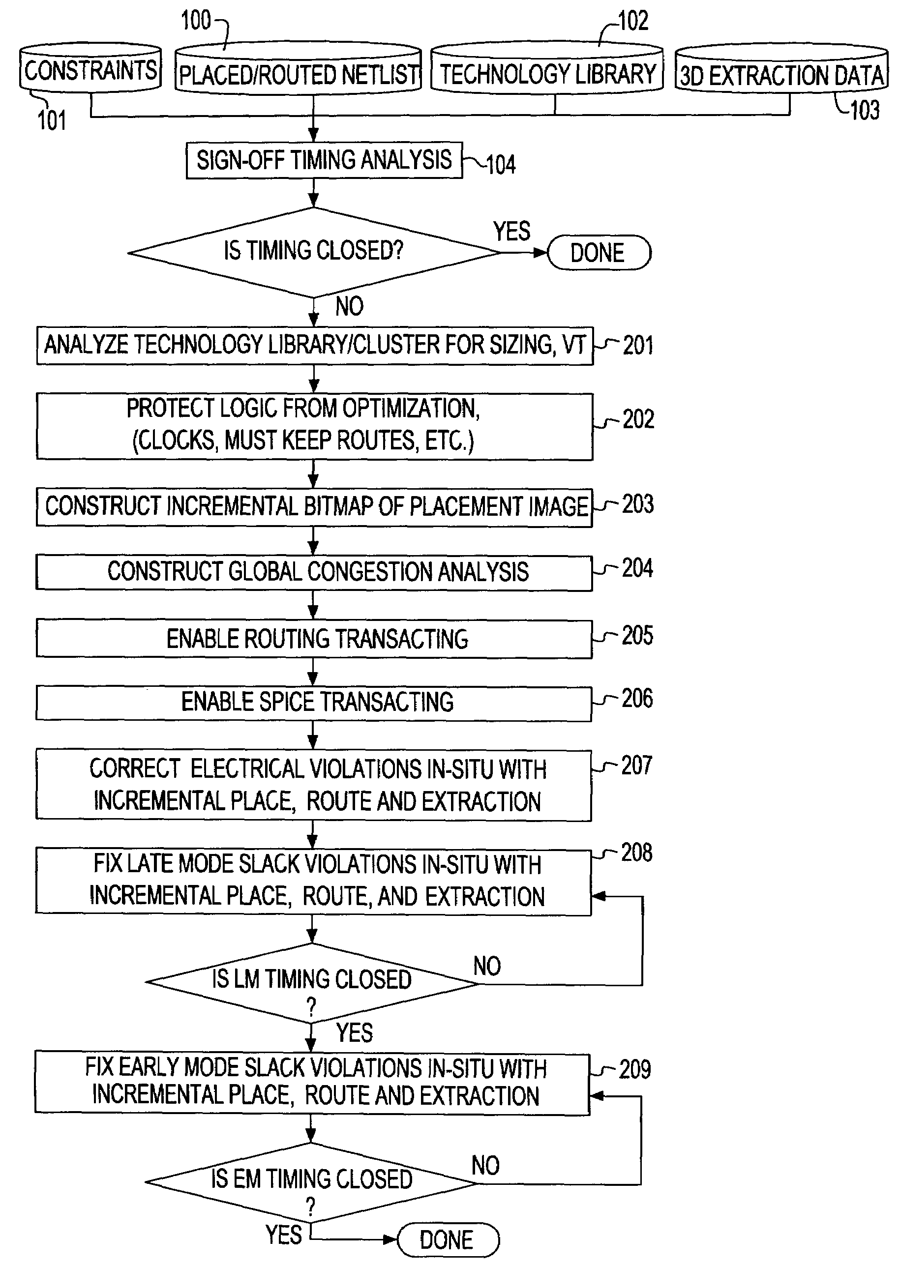
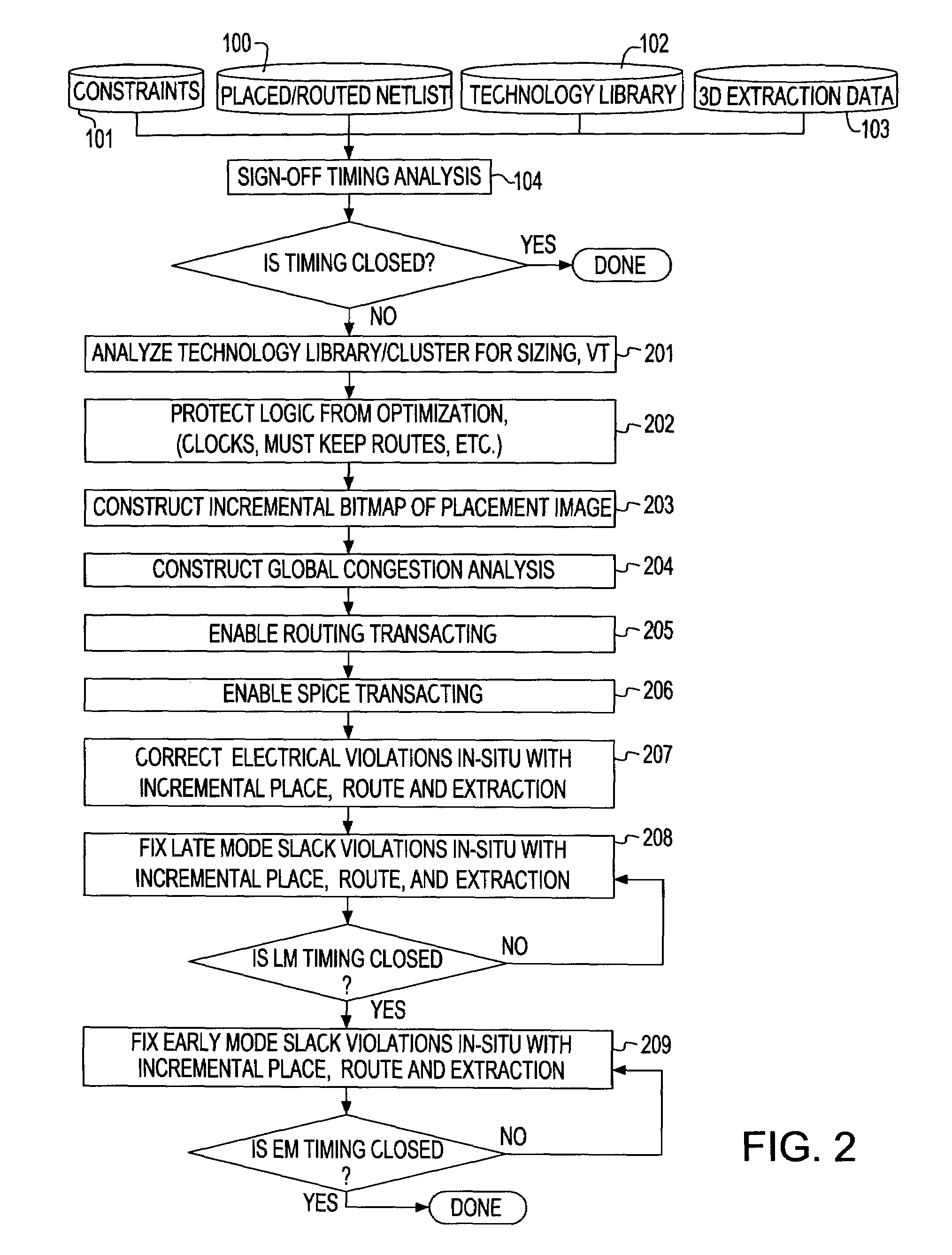
[0057]The present invention and the various features and aspects thereof are explained more fully with reference to non-limiting embodiments that are illustrated in the accompanying drawings and detailed in the following description.

[0058]In the description hereinafter described, the following definition of terms will be used.

[0059]Late mode—establishes the longest delay, or critical path, which sets the maximum speed at which the VLSI chip can run.

[0060]Early mode—determines the conditions that are necessary for a correct operation of the chip when fast paths resulting from signals arriving before expected are found to exist.

[0061]Transition time—defines the time it takes for a signal waveform to travel from 10% to 90% of its final value. It is also referred to as slew time.

[0062]Legal placement—defines a condition where every circuit of the design is placed according to placement rules and constraints. A circuit must be placed such that its occupying area does not overlap that of ...


PUM


Abstract

A method for performing timing optimization of a detail routed netlist, incorporating statistical variability information, common path pessimism reduction, and capacitative coupling information, in a tightly coupled, incremental manner with minimal perturbations to the placement, routing, and asserted parasitic information. The method corrects violations in a placed and routed design of a VLSI circuit chip, where the design is represented by a netlist describing logical and physical characteristics of the design and by a corresponding timing graph, the method including the steps of: identifying violations in the design; iteratively eliminating the violations by incrementally transforming the logical and the physical characteristics of the design, incorporating in the design only legal placements and routes; and applying incremental timing to evaluate the transformations, and updating the existing timing graphs to reflect changes consisting of the legal placements and routes.

Description

FIELD OF THE INVENTION[0001]The present invention is related to the design of Very Large Scale Integrated (VLSI) circuits, and more particularly, to a system and method for signing-off timing closure that guarantees the functionality and performance of a VLSI chip.DESCRIPTION OF THE PRIOR ART[0002]The trend of VLSI technologies has caused a marked increase in the amount of time it takes to close on-chip timing due to the increased need for accurate timing information to make optimization decisions and increasing feature sizes of chips. Parasitic extraction, capacitive coupling, and variability often cause perturbations that necessitate determining the exact capacitive and resistance effects of each layer for routes along interconnects in a netlist in order to provide a converging timing closure process.[0003]Today's process is manual in nature and does not provide an efficient feedback to the decision making, thereby creating new problems such as generating wiring congestion, overpo...

Claims


Application Information

Patent Timeline
Patent Type & Authority Patents(United States)
IPC IPC(8): G06F17/50
CPCG06F17/5068G06F2217/84G06F30/39G06F2119/12
Inventor KAZDA, MICHAEL A.KOTECHA, POOJA M.MATHENY, ADAM P.REDDY, LAKSHMITREVILLYAN, LOUISE H.VILLARRUBIA, PAUL G.
Owner INT BUSINESS MASCH CORP
Why Eureka
Try Eureka