Electronic package

a technology of electronic packaging and packaging components, applied in the field of electronic packaging, can solve the problems of increasing production cost, and achieve the effect of manufacturing with a lower production cos

Active Publication Date: 2009-09-08
ADVANCED SEMICON ENG INC
View PDF2 Cites 29 Cited by
  • Summary
  • Abstract
  • Description
  • Claims
  • Application Information

AI Technical Summary

Benefits of technology

[0009]It is an object of the present invention to provide an electronic package that can be manufactured with lower production cost.
[0011]In another preferred embodiment, at least one trench is further formed on the central protrusion. The trench can prevent the molten sealant from flowing through the gap between the mold and the central protrusion to the upper surface of the central protrusion during the formation of the second sealant.
[0012]The electronic packages of the present invention are characterized in that the second substrate has a central protrusion, and the bonding wires and sealant are positioned on the rim portion of the second substrate. In this way, there is no need to use the special mold for forming the sealant to encase the bonding wires. The ordinary mold can be used to form the sealant. Accordingly, the production cost can be greatly reduced. Besides, in the electronic packages of the present invention, only a conventional flat substrate is required to be replaced with a substrate having a central protrusion. There is no need to change the manufacturing process in order to form the electronic packages of the present invention.

Problems solved by technology

Such special mold is much expensive and thus leads to the increase in production cost.

Method used


Image

  • Electronic package
  • Electronic package
  • Electronic package

Examples


Embodiment Construction

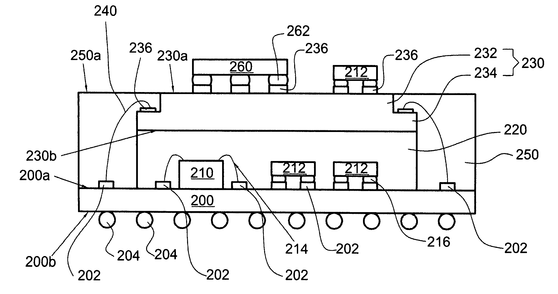
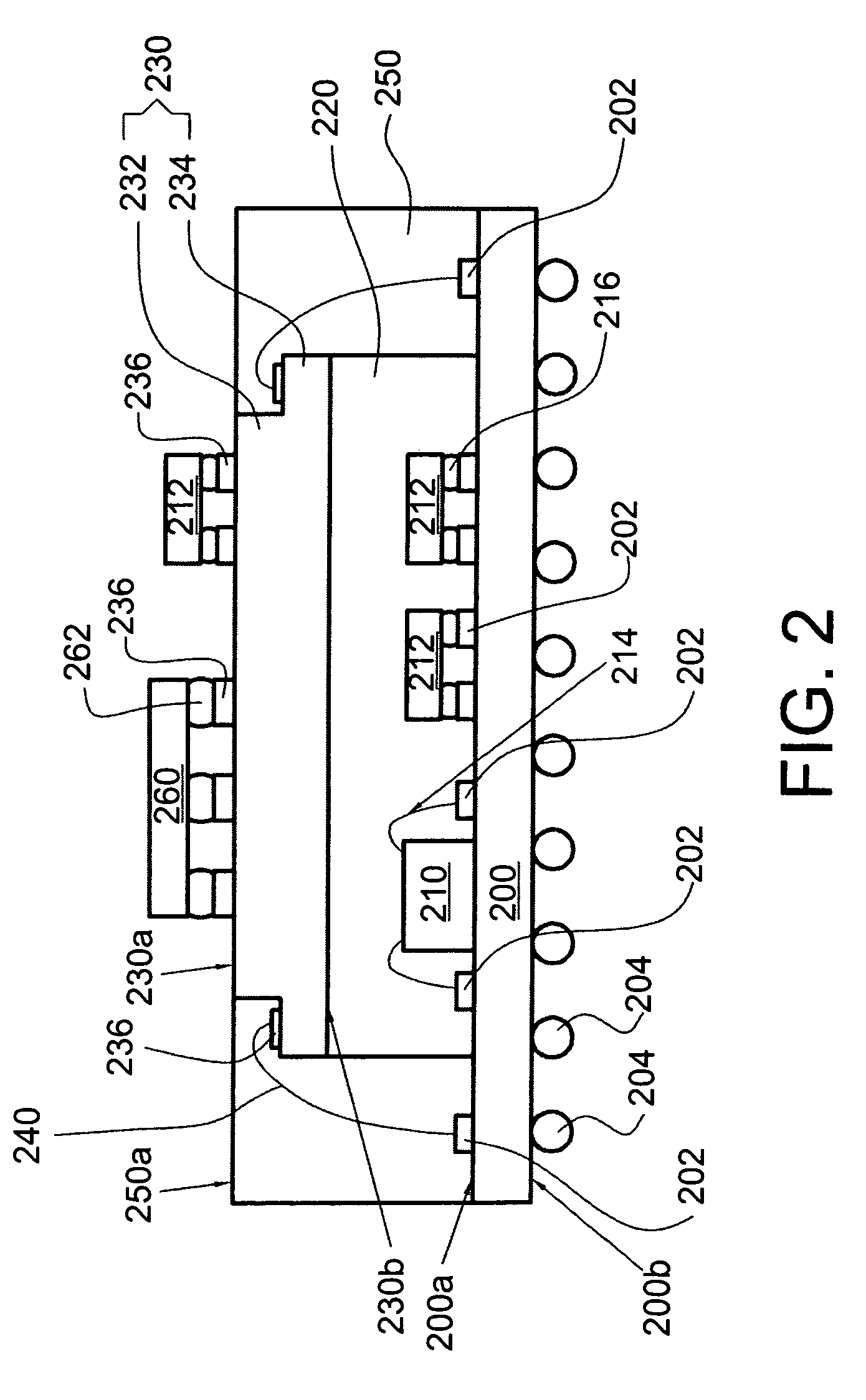
[0017]Referring to FIG. 2, it is a cross-sectional view of an electronic package according to a preferred embodiment of the present invention. The electronic package according to the preferred embodiment of the present invention at least includes a first substrate 200, a first electronic component such as an active component 210 or a passive component 212, a first sealant 220, a second substrate 230, a plurality of bonding wires 240, a second sealant 250 and a second electronic component such as a memory chip 260 or a passive component212, wherein the first substrate 200 has opposing upper surface 200a and lower surface 200b. A plurality of first bonding pads 202 is disposed on the upper surface 200a of the first substrate 200 and a plurality of metal bumps 204 is attached to the lower surface 200b of the first substrate 200. The first electronic component is positioned on the upper surface 200a of the first substrate 200 and electrically connected to the first bonding pads 202. In ...


PUM


Abstract

An electronic package is provided. The electronic package includes a first substrate, an electronic component, a first sealant, a second substrate, a plurality of bonding wires and a second sealant, wherein the first substrate has opposing upper and lower surfaces and a plurality of bonding pads is disposed on the upper surface of the first substrate. The electronic component is positioned on the upper surface of the first substrate and electrically connected to the bonding pads. The first sealant is formed on the upper surface of the first substrate to encapsulate the electronic component. The lower surface of the second substrate is attached to the first sealant. The upper surface of the second substrate includes a central protrusion and a rim portion which surrounds and is lower than the central protrusion. A plurality of bonding wires is used to electrically connect the rim portion to the first substrate. The second sealant is formed on the upper surface of the first substrate and on the rim portion of the second substrate to encapsulate the bonding wires, the first sealant and the rim portion.

Description

CROSS REFERENCE TO RELATED APPLICATION[0001]This application claims the priority benefit of Taiwan Patent Application Serial Number 095147735 filed Dec. 19, 2006, the full disclosure of which is incorporated herein by reference.BACKGROUND OF THE INVENTION[0002]1. Field of the Invention[0003]The invention relates to an electronic package, and more particularly, to an electronic package with a central protrusion on the substrate.[0004]2. Description of the Related Art[0005]As electronic products are getting smaller and lighter, the packages for protecting and interconnecting IC chips also have the same trend. With ever-increasing demands for miniaturization and higher operating speeds, multi-chip packages have become an attractive approach in a variety of electronic device. Multi-chip packages, which contain two or more chips in a single package, can help minimize the limitation in system operation speed. In addition, multi-chip packages are capable of decreasing the interconnection l...

Claims


Application Information

Patent Timeline
Patent Type & Authority Patents(United States)
IPC IPC(8): H01L23/498
CPCH01L25/162H05K1/144H01L24/16Y10T428/23H01L24/48H01L2224/16H01L2224/45144H01L2224/48091H01L2924/01079H01L2924/14H01L2924/1433H01L2924/15311H01L2924/1815H01L2924/19041H01L2924/19043H01L2924/19105H01L2924/19107H05K2201/042H05K2201/10977H05K2203/049H01L24/45H01L2924/00014H01L2924/181H01L2224/16225H01L2924/00011H01L2224/0401H01L2924/00012
Inventor HUNG, CHIH PINCHIU, CHI TSUNGOU, IN DEWANG, YUNG HUI
Owner ADVANCED SEMICON ENG INC
Why Eureka
Try Eureka