Alignment sensing method for semiconductor device

a technology of alignment sensing and semiconductor devices, which is applied in the direction of semiconductor devices, semiconductor/solid-state device details, instruments, etc., can solve the problems of decrease of alignment accuracy of fia, and uneven polishing of regions into hollows, etc., to achieve low deformation, high accuracy, and high contrast

Inactive Publication Date: 2009-09-08
KIOXIA CORP +1
View PDF9 Cites 2 Cited by
  • Summary
  • Abstract
  • Description
  • Claims
  • Application Information

AI Technical Summary

Benefits of technology

[0019]As described above, according to the present invention, a plurality of alignment marks formed on a semiconductor wafer are respectively divided by micronized...

Problems solved by technology

That is, a size of the alignment marks is too large in comparison with a size of the cell pattern, which hinders the upper surface of the region for the alignment marks formed in from being evenly polished, with a result that the region is often unevenly polished into a hollow like a dish.
In the step of forming a metal film by sputtering, the metal film is often unsymmetrically formed on both sides of the edges of the alignment marks.
In a case that a shape of alignment marks is deformed unsymmetrical through the above-described CMP step and the metal film forming step, a central position of the alignment marks cannot be sensed, and a metering error that ...

Method used


Image

  • Alignment sensing method for semiconductor device
  • Alignment sensing method for semiconductor device
  • Alignment sensing method for semiconductor device

Examples


first embodiment

A First Embodiment

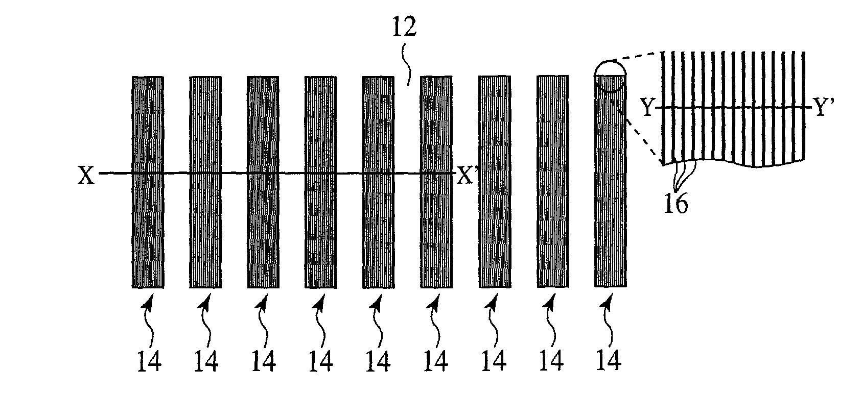
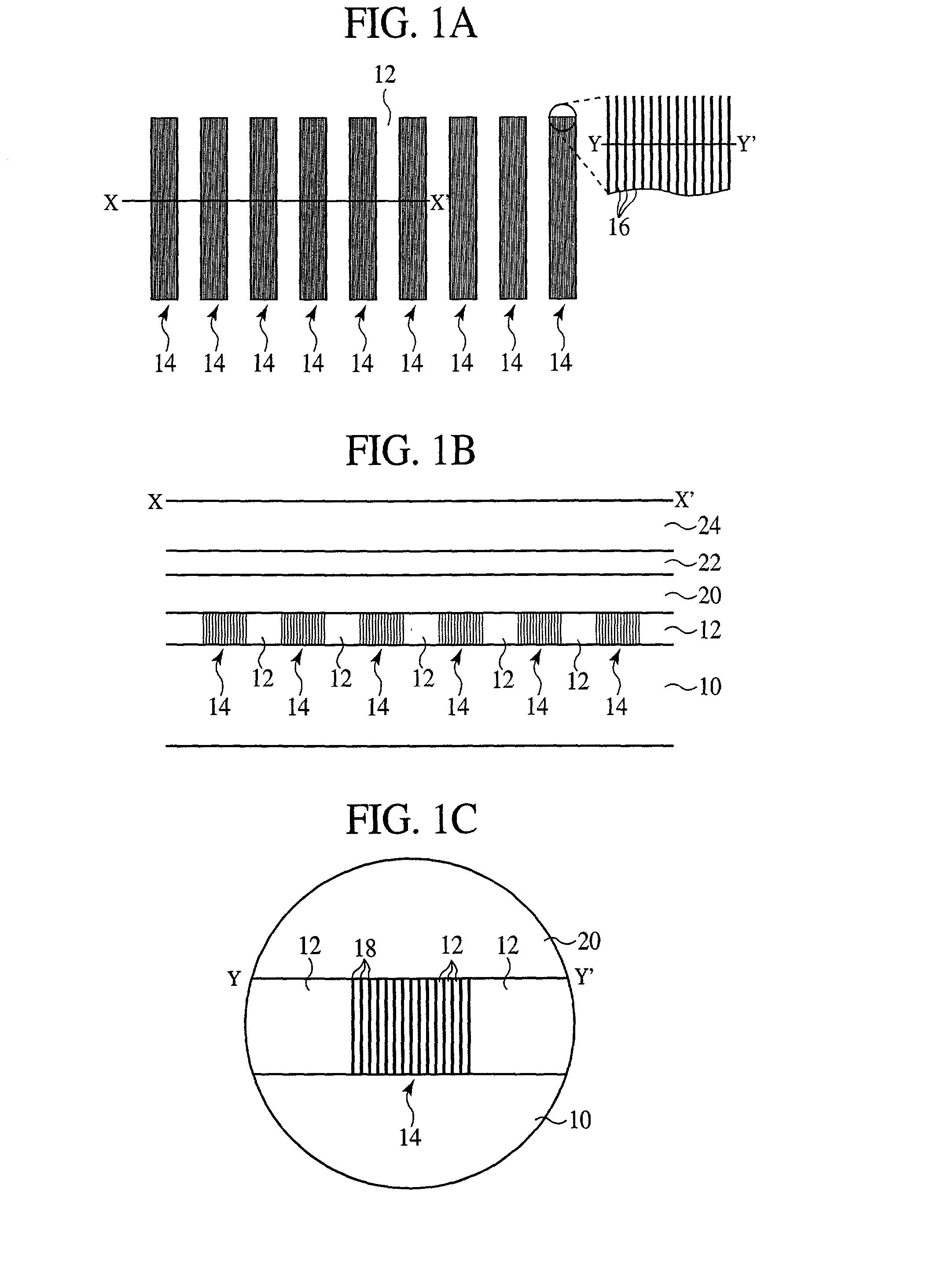
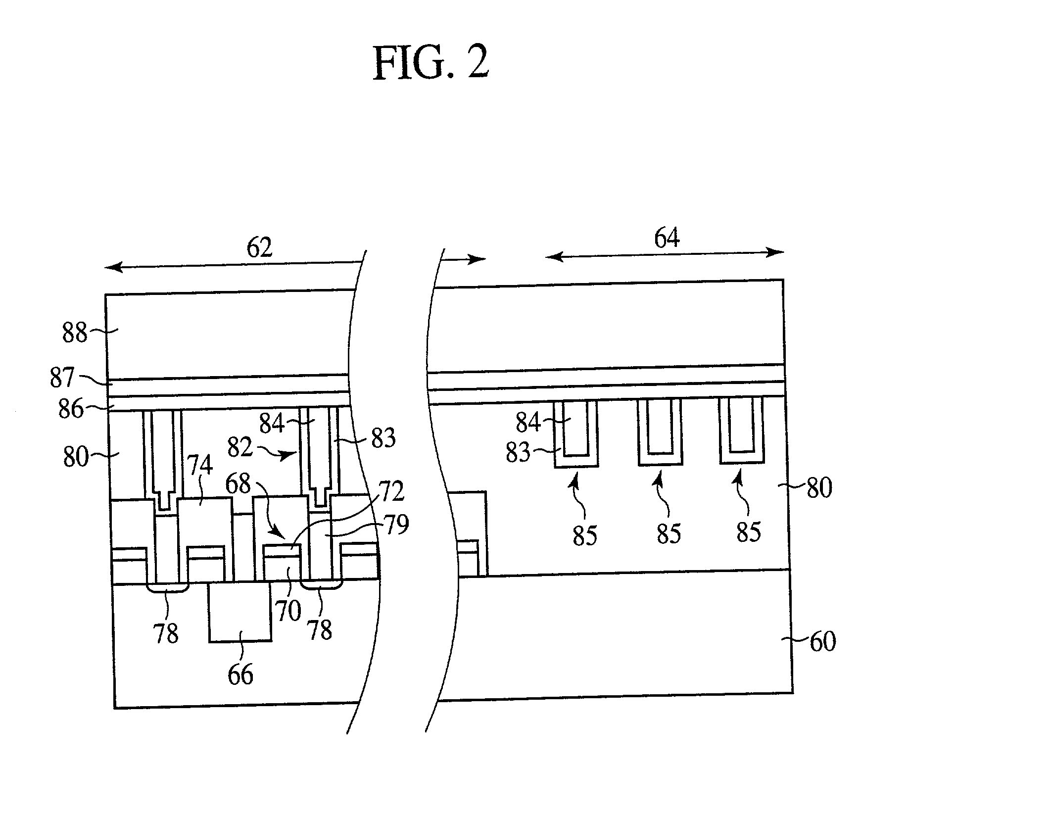
[0029]The semiconductor device and an alignment sensing method for the semiconductor device according to a first embodiment will be explained with reference to FIGS. 1A-1C, 2, 3, and 4. FIGS. 1A-1C are diagrammatic views of alignment marks of the semiconductor device according to the first embodiment, which show a structure of the alignment marks. FIG. 2 is a sectional view of the semiconductor device according to the present embodiment, which shows a structure thereof. FIG. 3 is a diagrammatic view of the alignment sensor, which shows a structure thereof. FIG. 4 is a graph of one example of FIA signals of the alignment marks of the semiconductor device according to the present embodiment.

[0030]First, a structure of the alignment marks of the semiconductor device according to the present embodiment will be explained with reference to FIGS. 1A-1C. FIG. 1A is a top view of the alignment marks of the semiconductor device according to the present embodiment. FIG. 1B is...

second embodiment

A Second Embodiment

[0064]The semiconductor device and the alignment sensing method according to a second embodiment of the present invention will be explained with reference to FIGS. 6A-6C and 7. FIGS. 6A-6C are diagrammatic views of alignment marks of the semiconductor device according to the present embodiment, which show a structure thereof. FIG. 7 is a graph of one example of FIA signals of the alignment marks of the semiconductor device according to the present embodiment. The same members of the present embodiment as those of the semiconductor device according to the first embodiment are represented by the same reference numbers not to repeat or to simplify their explanation.

[0065]It can be suppressed by dividing alignment marks to be near a size of a device pattern formed on a wafer that alignment marks are deformed to be unsymmetrical due to dishing or other causes in the conventional CMP step.

[0066]Alignment marks, which are positioned generally on scribe lines at an outer ...


PUM


Abstract

Strip-shaped alignment marks 14 are juxtaposed with each other in a silicon oxide film 12 formed on a silicon wafer 10. Each alignment mark 14 comprises a plurality of grooves 16 formed side by side in the silicon oxide film 12. An amorphous silicon film 18 is buried in the grooves 16. Thus, the alignment marks 14 are formed in a thus-formed line-and-space pattern. Accordingly, waveforms of detected signals having high contrast and little deformation can be obtained, and alignment of wafers with high accuracy can be realized.

Description

BACKGROUND OF THE INVENTION[0001]The present invention relates to a semiconductor device having alignment marks to be used in aligning the semiconductor device by an aligner.[0002]A process for fabricating a semiconductor device includes a lithography step of forming a device pattern on a wafer, as of silicon or others.[0003]In the lithography step, first, a resist is applied by a spin coater or others to a conducting layer or an insulation film laid on a wafer. Then, a mask having dimensions or a layout of a device drawn on is exposed by an aligner, such as a stepper, a scanner or others, in alignment with a prescribed position. Thus, the pattern of the mask is transferred to the resist film. Accuracy of the alignment of the wafer in the transfer by exposing the device pattern is an important element on which production yields of products depend on.[0004]As a method for aligning a wafer in an aligner, FIA (Field Image Alignment), for example is known. An alignment sensor of FIA met...

Claims


Application Information

Patent Timeline
IPC IPC(8): H01L23/544G03F9/00H01L21/027
CPCH01L23/544H01L2223/54453H01L2223/54426H01L2223/5442H01L2924/0002H01L2924/00
Inventor HOSHI, KENJINOMURA, HIROSHIISHIBASHI, SHIGERUSHI, YI-YU
Owner KIOXIA CORP
Why Eureka
Try Eureka