
Device for final inspection

a technology for semiconductor components and devices, applied in measurement devices, electrical testing, instruments, etc., can solve the problem that no oxide can form on the metal surface of contact pins, and achieve the effect of improving the service life of contact pins and improving the measurement reliability of test devices

Active Publication Date: 2009-09-15
ATMEL CORP
View PDF15 Cites 2 Cited by
  • Summary
  • Abstract
  • Description
  • Claims
  • Application Information

AI Technical Summary

Benefits of technology

This approach significantly reduces contact resistance and prevents oxide formation, thereby increasing the service life of contact pins and improving measurement reliability by maintaining a consistent inert environment, even at varying temperatures.

Problems solved by technology

Secondly, no oxide can form on the metal surfaces of the contact pin points because of the inert atmosphere.

Method used


Image

  • Device for final inspection
  • Device for final inspection
  • Device for final inspection

Examples


Embodiment Construction

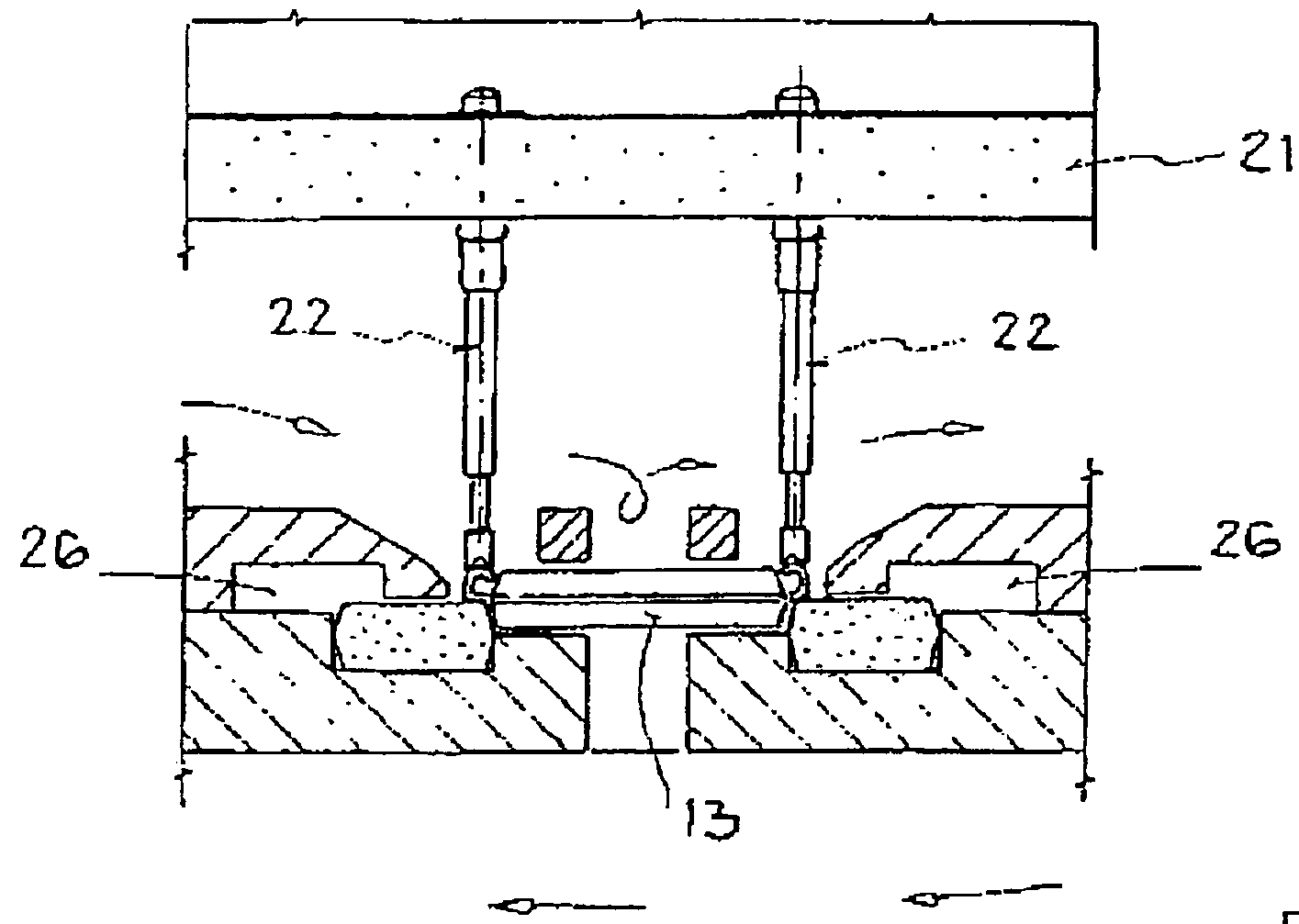
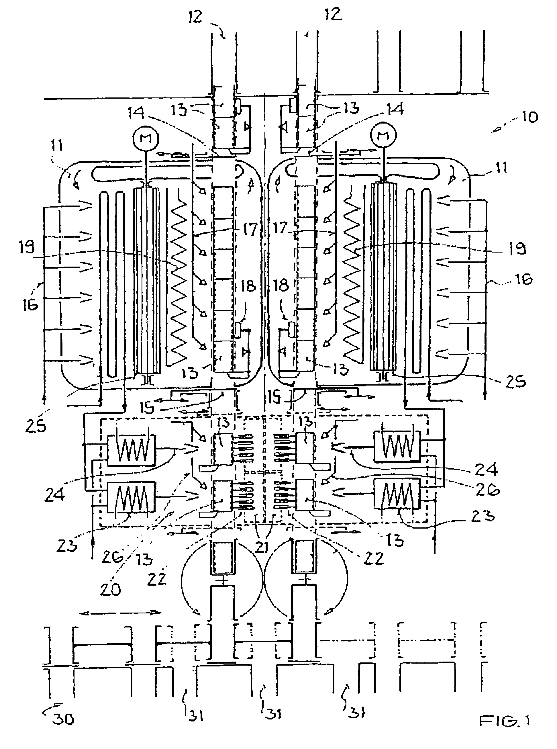
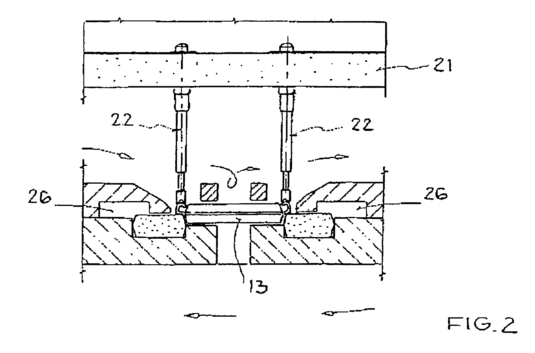
[0034]FIG. 1 shows an environmental chamber 10 of a handler with a left-hand and a right-hand holding chamber 11. Singulated ICs 13 are supplied to the environmental chamber 10 through loading devices 12. The holding chambers 11 are each closed off from the open areas of the handler by a chamber entry closure 14 and a chamber exit closure 15 in order to heat or cool the ICs 13 for testing to a defined test temperature.

[0035]Three temperature ranges are distinguished. During testing at low temperatures, which takes place at approximately −40° C., liquid nitrogen is supplied to the holding chambers 11 through separate lines and nozzles 16. Normally, temperature regulation of the ICs 13 is accomplished under program control, so no influences can act on the atmosphere inside the environmental chamber 10. Transport of the ICs 13 inside the environmental chamber 10 takes place by means of a pneumatically controlled device with lines and nozzles 17. In addition, holding devices 18 are loca...


PUM


Abstract

A device is provided for subjecting a plurality of singulated semiconductor components to functional verification, which includes contact pins that are integrated in a test socket and establish a mechanical and electrical contact between the test socket and the integrated semiconductor circuits, a holding fixture (DUT board) connected to the test socket for transmitting electrical signals to and from a program-controlled electronic switching system, and lines and control devices for operating at least one pneumatic transport and holding device for picking up, orienting and positioning the singulated semiconductor components, an inert gas is provided as the medium for operating the pneumatic devices.

Description

[0001]This nonprovisional application claims priority to German Patent Application No. DE 102006009321, which was filed in Germany on Mar. 1, 2006, and to U.S. Provisional Application No. 60 / 781,382, which was filed on Mar. 13, 2006, and which are both herein incorporated by reference.BACKGROUND OF THE INVENTION[0002]1. Field of the Invention[0003]The present invention relates to a device for testing various semiconductor components, including integrated semiconductor circuits, known as ICs (integrated circuits).[0004]2. Description of the Background Art[0005]After integrated semiconductor circuits have been singulated, they undergo functional verification in a test step. To this end, ICs are brought into contact with test sockets in a test device in order to test the individual components for functionality. These test devices are usually called “IC testers” or “IC handlers.”[0006]Although the invention is described below with reference to ICs as typical semiconductor components, it...

Claims


Application Information

Patent Timeline
Patent Type & Authority Patents(United States)
IPC IPC(8): G01R31/02
CPCG01R31/2881G01R31/2862
Inventor HEINKE, MATTHIASWIECZOREK, HEINRICH
Owner ATMEL CORP
Learn More