Solution synthesis of germanium nanocrystals

a technology of nanocrystals and nanowires, applied in metal-working apparatuses, transportation and packaging, etc., can solve the problems of difficult separation and purification processes, difficult control of the ge nc surface, and inability to find suitable solution synthesis routes for group iv ncs,

Active Publication Date: 2009-09-22
NAT TECH & ENG SOLUTIONS OF SANDIA LLC
View PDF11 Cites 5 Cited by
  • Summary
  • Abstract
  • Description
  • Claims
  • Application Information

AI Technical Summary

Problems solved by technology

However, suitable solution synthesis routes for Group IV NCs, such as Si and Ge, are not readily available even though Si and Ge are two important semiconductor materials and have been widely used in microelectronics, power g

Method used


Image

  • Solution synthesis of germanium nanocrystals
  • Solution synthesis of germanium nanocrystals
  • Solution synthesis of germanium nanocrystals

Examples


Embodiment Construction

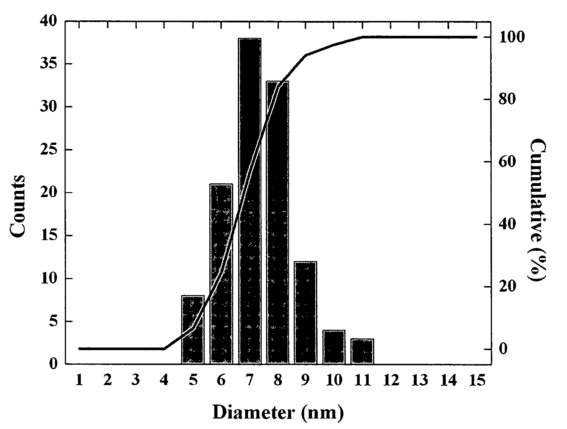
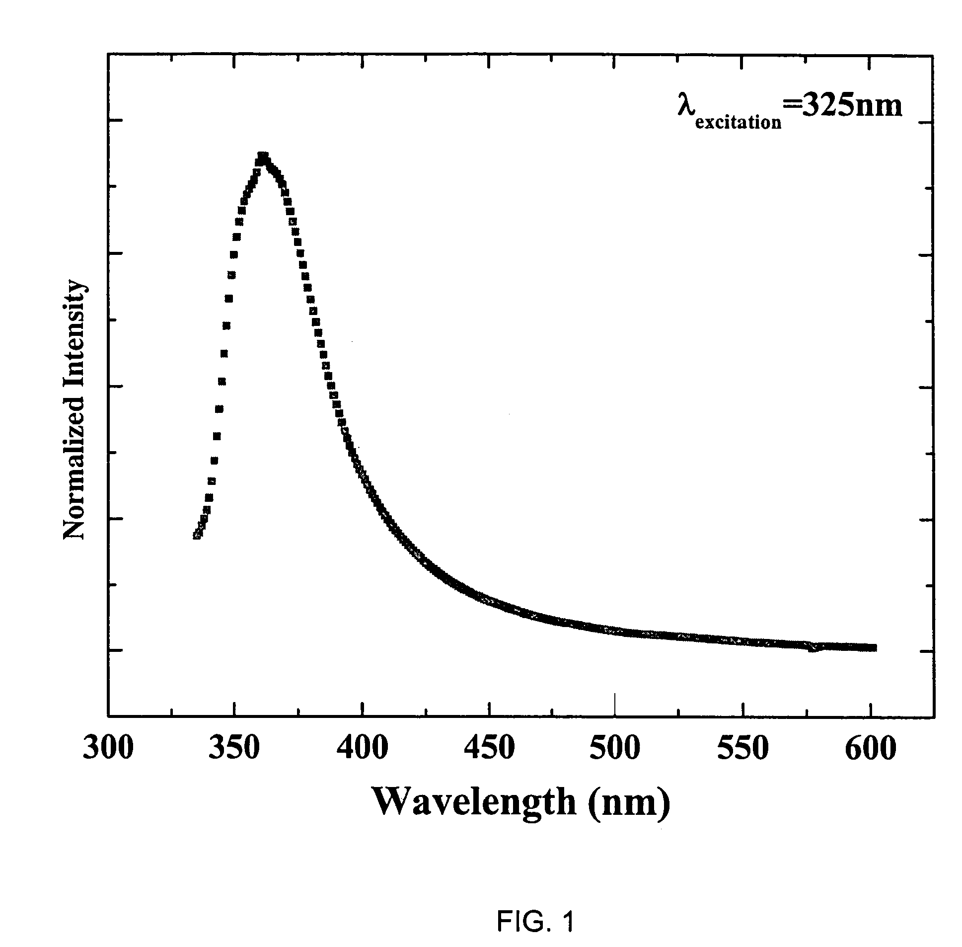
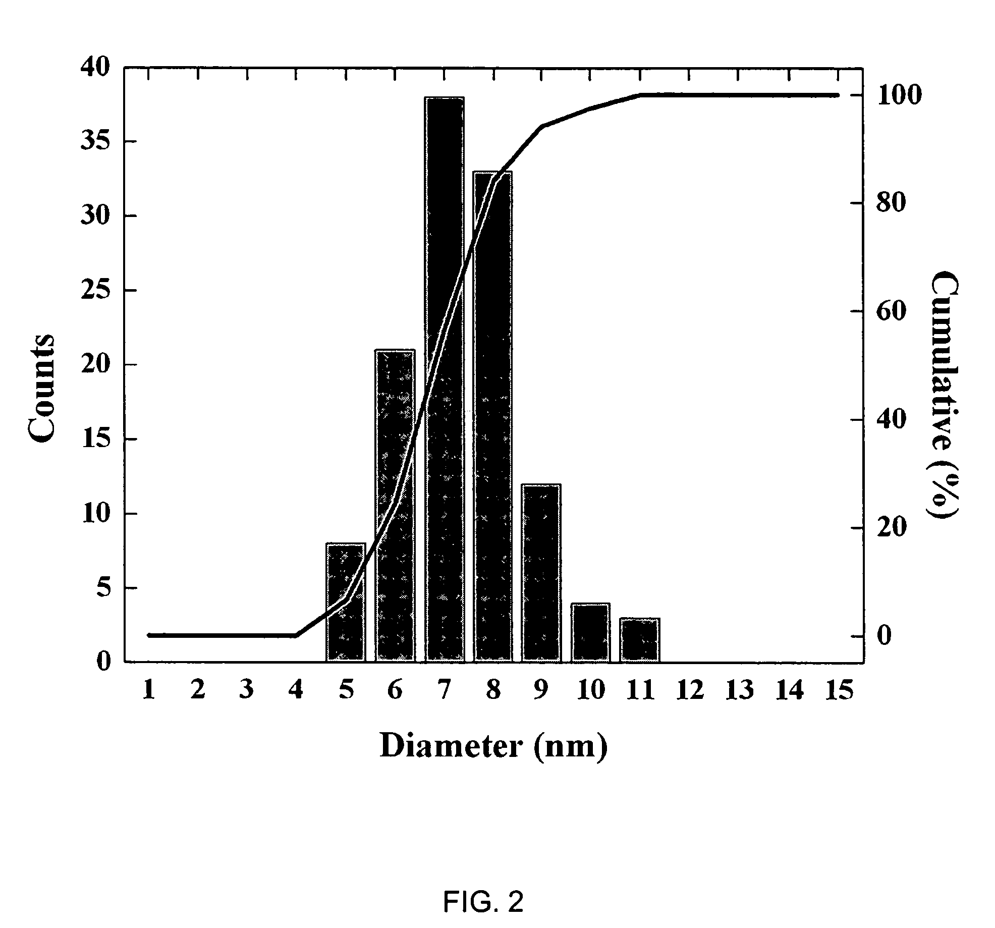
[0011]The present invention relates to a thermal reduction method for synthesizing Ge(0) nanometer-sized materials, comprising either Ge(0) nanocrystals or Ge(0) nanowires. As used herein, “nanocrystals” and “nanowires” define a crystalline domain having dimensions along at least one axis of between 1 nanometer and 100 nanometers and “nanomaterials” refers to nanometer-sized nanocrystals or nanowires or both.

[0012]The method involves thermal reduction of a Ge(II) precursor compound to the Ge(0) nanometer-sized material. To form a Ge(0) nanomaterial, a Ge(II) precursor compound is dissolved in a ligand heated to a temperature sufficient to thermally reduce the Ge(II) to Ge(0), where the ligand can be any compound that can bond to the surface of the germanium nanomaterials to subsequently prevent agglomeration of the nanomaterials. This temperature is dependent upon the Ge(II) precursor and ligand compounds used but is generally between approximately 100° C. and 400° C. In an alternat...


PUM

PropertyMeasurementUnit
Temperatureaaaaaaaaaa
Size distributionaaaaaaaaaa

Abstract

A method for providing a route for the synthesis of a Ge(0) nanometer-sized material from. A Ge(II) precursor is dissolved in a ligand heated to a temperature, generally between approximately 100° C. and 400° C., sufficient to thermally reduce the Ge(II) to Ge(0), where the ligand is a compound that can bond to the surface of the germanium nanomaterials to subsequently prevent agglomeration of the nanomaterials. The ligand encapsulates the surface of the Ge(0) material to prevent agglomeration. The resulting solution is cooled for handling, with the cooling characteristics useful in controlling the size and size distribution of the Ge(0) materials. The characteristics of the Ge(II) precursor determine whether the Ge(0) materials that result will be nanocrystals or nanowires.

Description

[0001]This invention was made with Government support under Contract No. DE-AC04-94AL85000 awarded by the Department of Energy. The Government has certain rights in the invention.BACKGROUND OF THE INVENTION[0002]The present invention relates generally to a method of making germanium nanocrystals and nanowires, and, more particularly, to a method of making germanium nanocrystals and nanowires from germanium (II) precursors.[0003]Nanometer-sized crystalline semiconductor materials have potential applications in optoelectronics, photovoltaics, and biological imaging. These applications are based on the size-dependent quantum confinement effect, which is found in these nanostructure materials. Hence, the ability to control the size of these nanometer-size materials is import in the control of the material electronic and optical properties.[0004]Large-scale solution synthesis routes for compound semiconductor nanocrystals (NCs) such as CdSe, CdS, CdTe, PbSe, ZnO, InP, and AgBr are availa...

Claims


Application Information

Patent Timeline
IPC IPC(8): B22F9/24
CPCB22F9/24B22F1/0014B22F1/0018B22F1/0025B22F2998/00B22F2999/00B22F2203/11B22F1/052B22F1/0547B22F1/054
Inventor GERUNG, HENRYBOYLE, TIMOTHY J.BUNGE, SCOTT D.
Owner NAT TECH & ENG SOLUTIONS OF SANDIA LLC
Why Eureka
Try Eureka