Etchants and etchant systems with plural etch selectivities

a technology of etch selectivities and etchants, applied in the direction of coatings, decorative arts, electrical equipment, etc., can solve the problems of reducing the etch rate of silicon nitride, difficult to etch an oxidized silicon nitride structure using phosphoric acid, and phosphoric acid is unable to significantly etch silicon nitride, so as to achieve the effect of minimizing the removal of desired isolation regions

Inactive Publication Date: 2009-09-22
MICRON TECH INC
View PDF23 Cites 13 Cited by
  • Summary
  • Abstract
  • Description
  • Claims
  • Application Information

AI Technical Summary

Benefits of technology

[0010]The present invention provides a method of removing an oxidized silicon nitride layer from an IC device once it has served its purpose during fabrication. While removing the oxidized silicon nitride layer, the inventive method minimizes removal of desired isolation regions from the IC device. The method uses a two step process: one step to remove the oxidized portion of the oxidized silicon nitride layer; and a second step to remove the silicon nitride portion of the oxidized silicon nitride layer. In removing the oxidized silicon nitride layer, the method uses an acid solution exhibiting a positive etch selectivity or ability to etch one material (i.e., silicon nitride) faster than a second material (i.e., silicon oxide).
[0012]The present invention yields several advantages over the prior art. One advantage is that the etch selectivity for silicon oxide-silicon nitride composite structures is improved, resulting in better geometry for further IC device processing. Another advantage, at least when the same acid is used as the first and the second etchant, is that the complexity and cost of the manufacturing process decreases because less wafer processing is necessary, i.e., separate rinsing and drying steps are not required.

Problems solved by technology

At low temperatures, phosphoric acid is unable to significantly etch the silicon nitride because of its inability to appreciably attack the silicon oxide.
Higher temperatures speed up the attack of the silicon oxide, but decrease the etch rate of the silicon nitride.
As a result, it has been difficult to etch an oxidized silicon nitride structure using phosphoric acid.
But adding fluoroboric acid has not significantly improved the ability of phosphoric acid to etch the oxidized silicon nitride structure without also attacking and degrading the oxide isolation regions.
Unfortunately, the selectivity of HF acid is negative or, in other words, HF acid severely etches silicon oxide to the extent of removing silicon oxide at a rate faster than silicon nitride, producing unfavorable geometry for further IC device processing.
When a field oxide region is present, the negative etch selectivity removes large amounts of the field oxide region, thus impairing the ability of the field oxide to act as an isolating region.
Too little removal by the HF acid prevents the phosphoric acid from attacking the silicon nitride, while too much removal by the HF acid unduly depletes the oxide isolation regions.
Etching with HF acid followed by phosphoric acid, however, also increases the materials used—each HF and H3PO4 etching step is followed by a rinsing and drying step, thus increasing the complexity and cost of the fabrication process.

Method used


Image

  • Etchants and etchant systems with plural etch selectivities
  • Etchants and etchant systems with plural etch selectivities
  • Etchants and etchant systems with plural etch selectivities

Examples


example

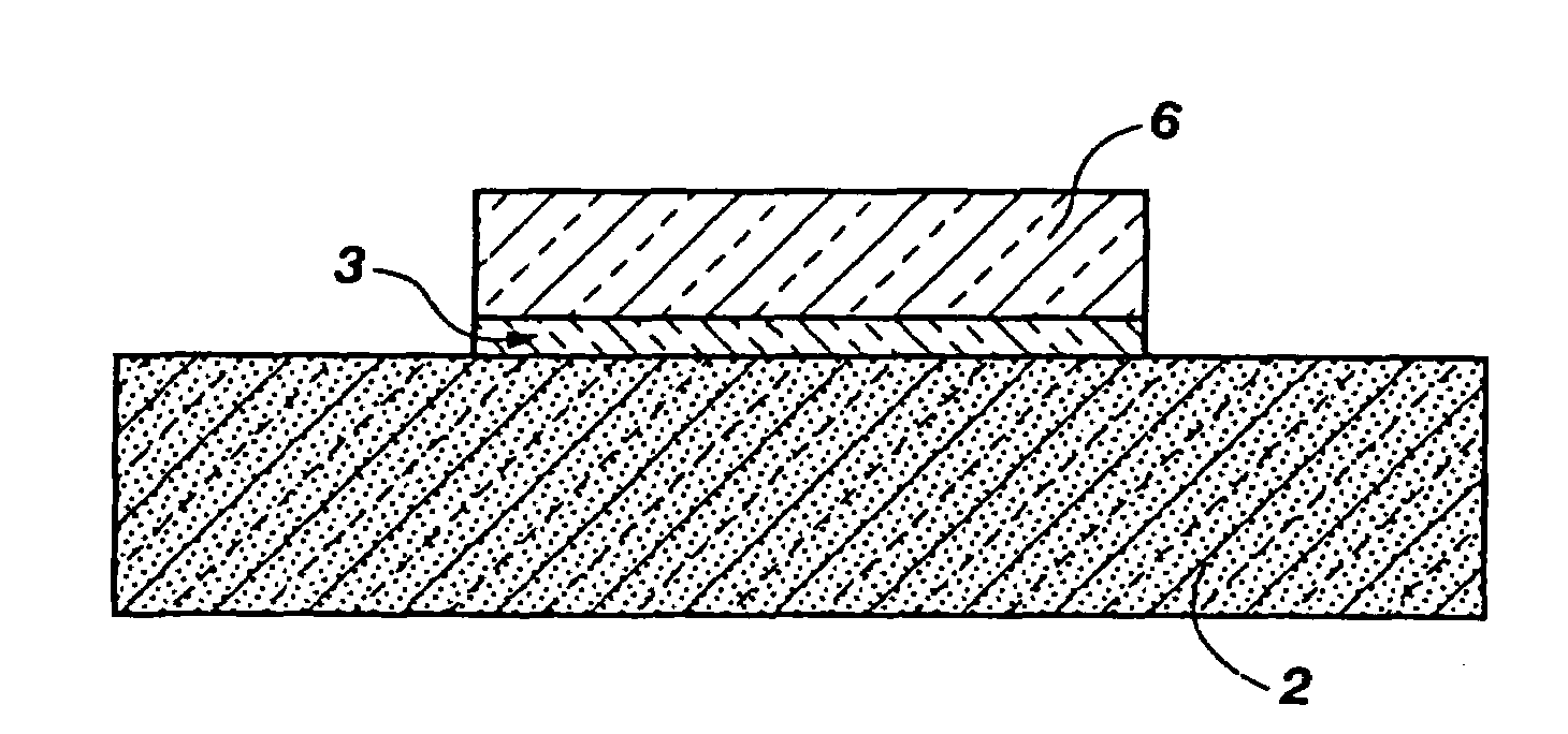
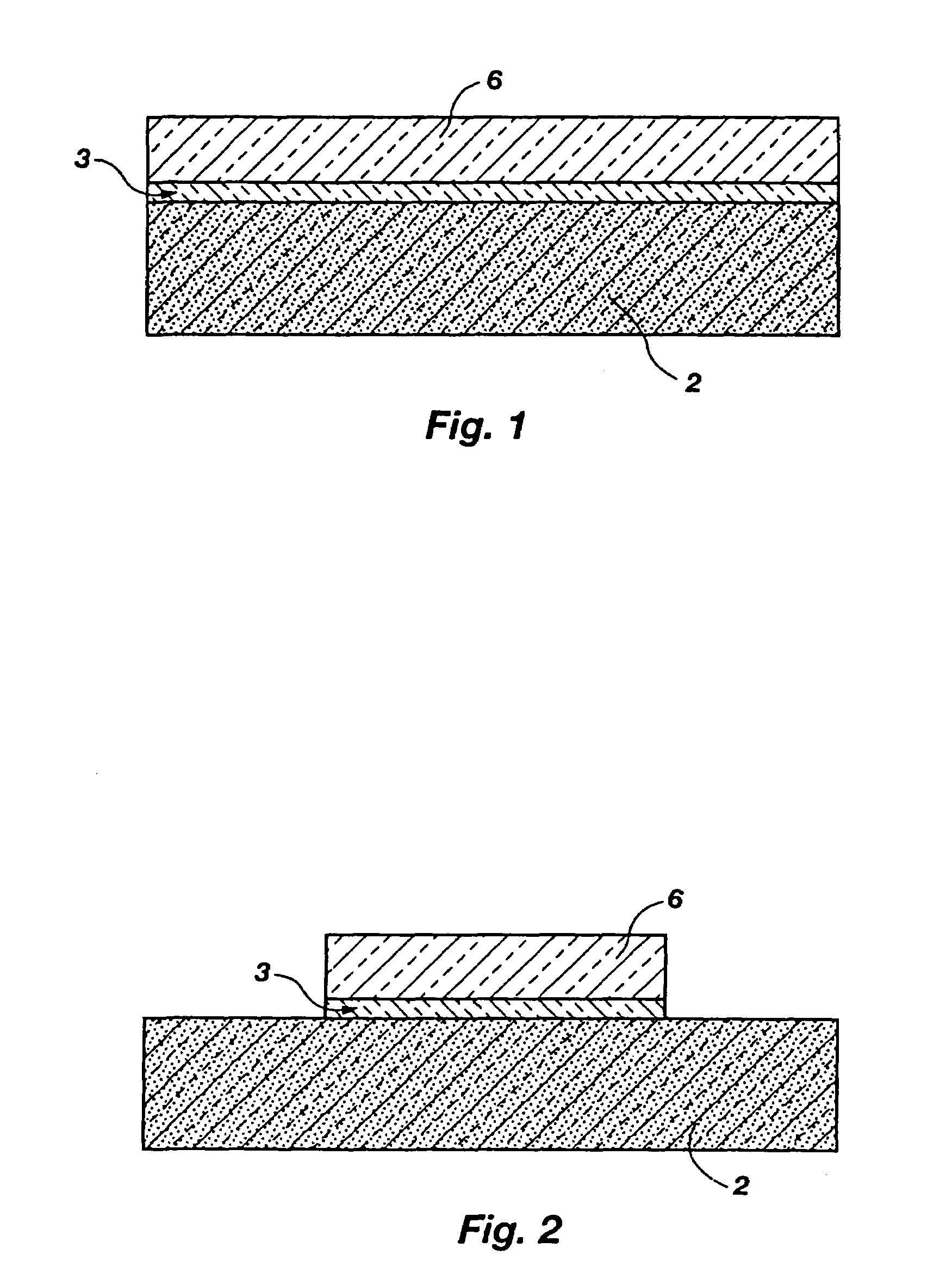
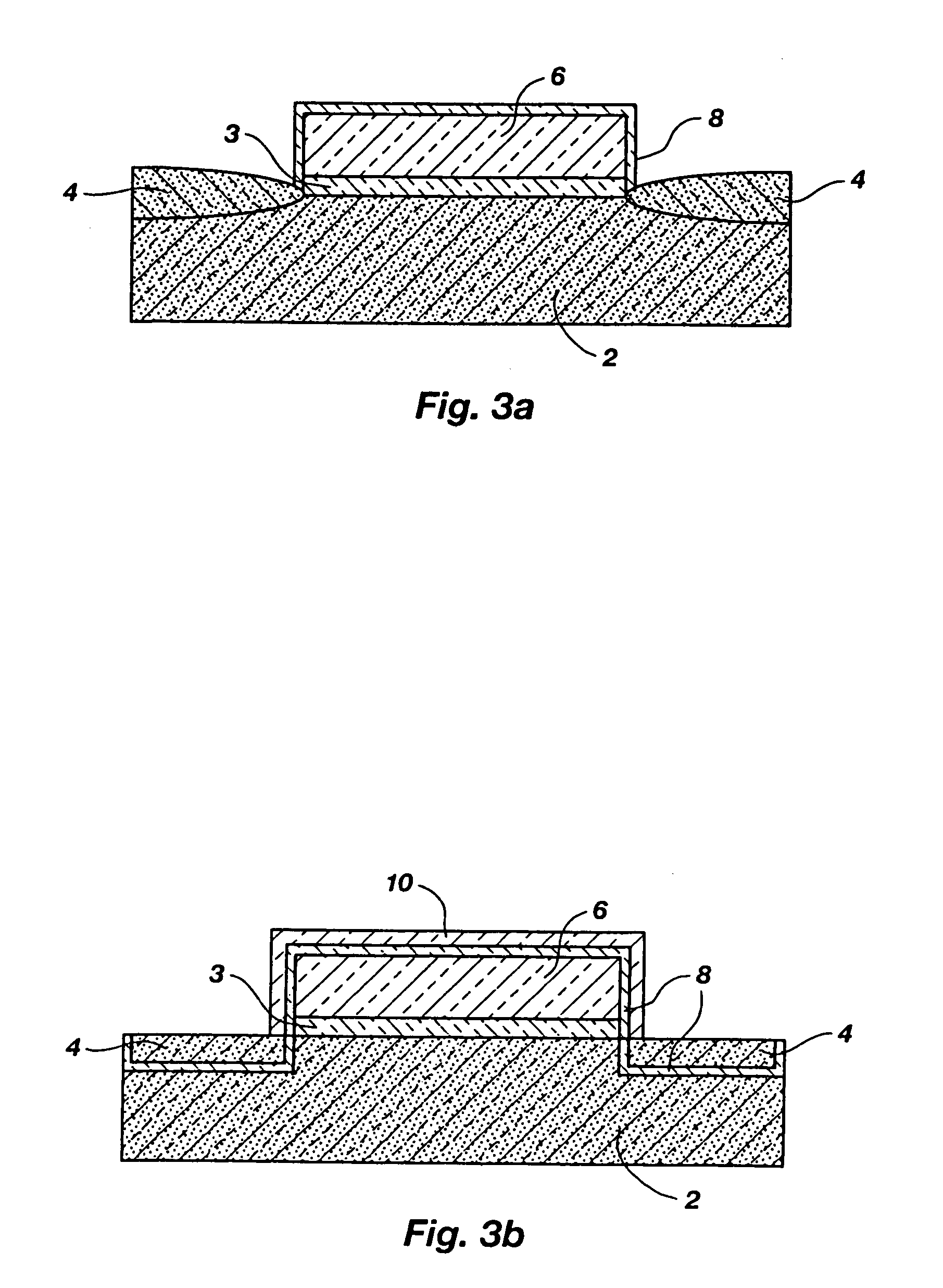
[0034]The preferred inventive method of using phosphoric acid at a first, higher temperature in a first step and then at a second, lower temperature in a second step was compared with using a conventional method of using HF acid in a first step and then using phosphoric acid in a second step. In both instances, after forming a thin pad oxide layer on a silicon substrate, a silicon nitride layer was deposited on the pad oxide layer. The silicon nitride and pad oxide layers were then patterned and etched. Field oxide regions with a thickness of 2200 angstroms were then formed by thermal oxidation in the substrate, also thermally oxidizing the silicon nitride layer.

[0035]The oxidized surface layer and underlying silicon nitride layer were then removed. Using the conventional HF acid in a first step and phosphoric acid in a second step to remove the oxidized surface layer and underlying silicon nitride layer resulted in about 240-260 angstroms of the field oxide regions also being remov...


PUM

PropertyMeasurementUnit
temperatureaaaaaaaaaa

Abstract

An etchant for removing materials with a plurality of selectivities exhibits a first etch selectivity at a first temperature and a second etch selectivity at a second temperature. The etchant may include phosphoric acid, fluoboric acid, or sulfuric acid. The materials that the etchant is configured to remove may include dielectric materials, such as silicon nitride and silicon oxide. The first temperature may be about 175° C. and the second temperature may be about 155° C.

Description

CROSS-REFERENCE TO RELATED APPLICATIONS[0001]This application is a divisional of U.S. patent application Ser. No. 10 / 837,920, filed May 3, 2004, pending, which is a continuation of U.S. patent application Ser. No. 10 / 327,375, filed Dec. 20, 2002, now U.S. Pat. No. 6,740,248, issued May 25, 2004, which is a continuation of U.S. patent application Ser. No. 09 / 518,292, filed Mar. 3, 2000, now U.S. Pat. No. 6,497,827, issued Dec. 24, 2002, which is a continuation of U.S. patent application Ser. No. 09 / 055,644, filed Apr. 6, 1998, now U.S. Pat. No. 6,117,351, issued Sep. 12, 2000.BACKGROUND OF THE INVENTION[0002]1. Field of the Invention[0003]This invention relates generally to the field of semiconductor design and fabrication. Specifically, the invention relates to methods for removing dielectric layers from integrated circuit devices.[0004]2. Background of Related Art[0005]During manufacture of integrated circuit (IC) devices, dielectric layers are often used to aid the fabrication pro...

Claims


Application Information

Patent Timeline
Patent Type & Authority Patents(United States)
IPC IPC(8): C23F1/00H01L21/311H01L21/32H01L21/762
CPCC03C15/00C03C17/22H01L21/76202H01L21/31111H01L21/32C03C2218/32C03C2218/33
Inventor LI, LIYATES, DON L.
Owner MICRON TECH INC
Why Eureka
Try Eureka