
Structure and Method for Forming a Salicide on the Gate Electrode of a Trench-Gate FET

a gate electrode and trench-gate technology, applied in the field of semiconductor technology, can solve the problems of increasing gate resistance, difficult to remove salicide formed on mesa surfaces, and reducing the cross-sectional area of salicide layers

Active Publication Date: 2010-09-30
SEMICON COMPONENTS IND LLC
View PDF27 Cites 8 Cited by
  • Summary
  • Abstract
  • Description
  • Claims
  • Application Information

AI Technical Summary

Benefits of technology

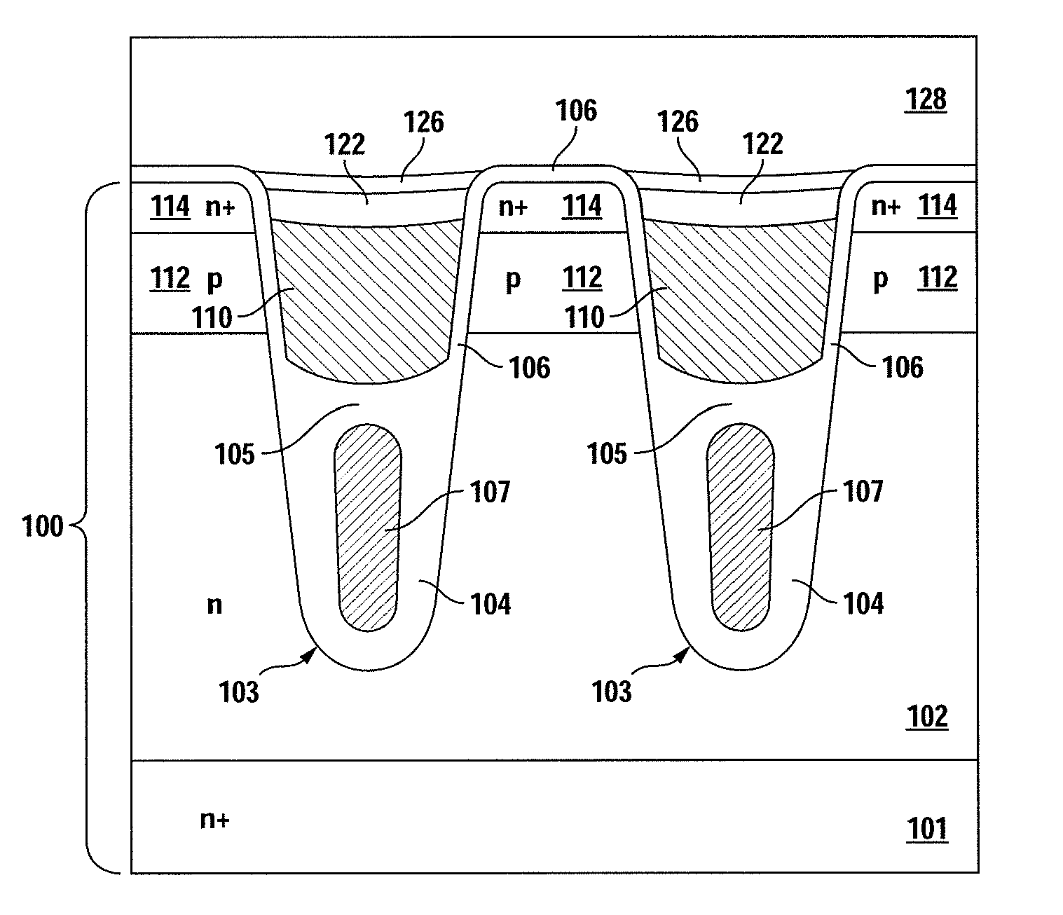
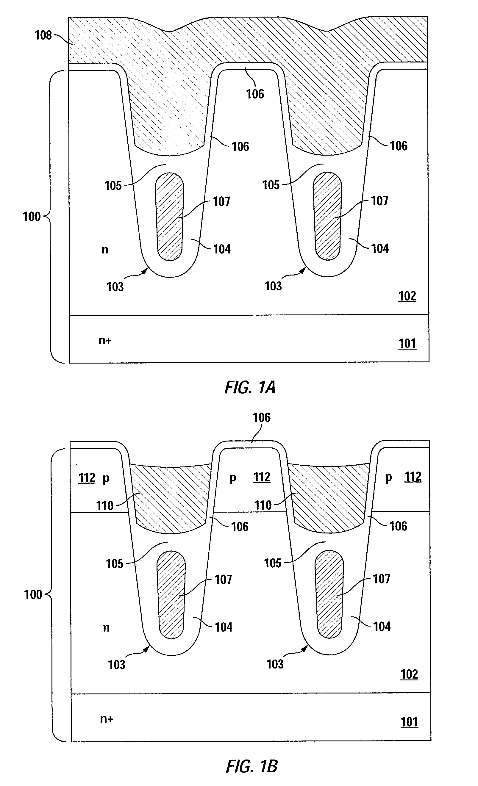
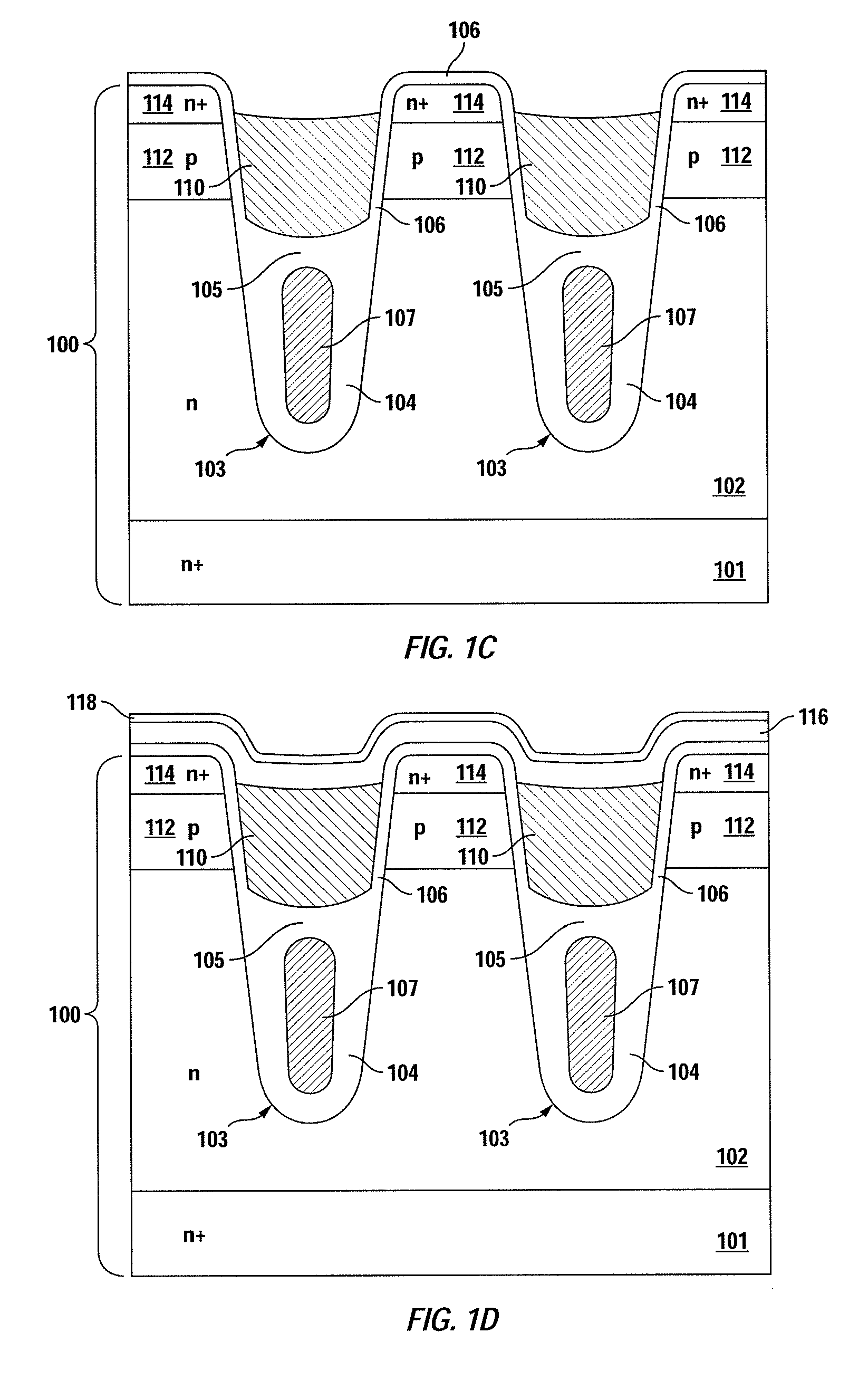
[0006]In accordance with an embodiment of the invention, trench-gate FET structures may be formed as follows. A plurality of trenches is formed extending into a semiconductor region. A gate dielectric is formed extending along opposing sidewalls of each trench and over mesa surfaces of the semiconductor region between adjacent trenches. A gate electrode is formed in each trench isolated from the semiconductor region by the gate dielectric. Well regions of a second conductivity type are formed in the semiconductor region. Source regions of the first conductivity type are formed in upper portions of the well regions. After forming the source regions, a salicide layer is formed comprising at least one of cobalt or nickel over the gate electrode in each trench abutting portions of the gate dielectric. The gate dielectric prevents formation of the salicide layer over the mesa surfaces of the semiconductor region between adjacent trenches.
[0010]In yet another embodiment, a wet clean process is performed without HF to minimize removal of exposed portions of the gate dielectric.

Problems solved by technology

Also, titanium salicide growth is isotropic, and the salicide layer can extend laterally causing bridging.
Using spacers, however, reduces the cross-sectional area of the salicide layer thus increasing gate resistance.
Salicide formed on the mesa surfaces is difficult to remove thus impacting subsequent contact etch processes.

Method used


Image

  • Structure and Method for Forming a Salicide on the Gate Electrode of a Trench-Gate FET
  • Structure and Method for Forming a Salicide on the Gate Electrode of a Trench-Gate FET
  • Structure and Method for Forming a Salicide on the Gate Electrode of a Trench-Gate FET

Examples


Embodiment Construction

[0017]In accordance with embodiments of the present invention, trench-gate FET structures with reduced gate resistance are obtained using simple manufacturing processes. Some embodiments include forming a salicide layer comprising cobalt or nickel over the gate electrode. Cobalt and nickel do not react with the silicon in silicon oxide to form stringers in the same manner as titanium, and thus spacers can be eliminated. Eliminating spacers increases the cross-sectional area of the salicide layer thus reducing gate resistance. Other embodiments include forming the source and well regions prior to salicide formation. Source and well formation require high temperature processing. Salicide layers have generally low thermal stability, and forming the salicide layer after source and well formation prevents exposure of the salicide layer to the high temperature processing. Other embodiments include forming source and well regions using thermal processes substantially without oxygen to mini...


PUM


Abstract

A method for forming a trench-gate FET includes the following steps. A plurality of trenches is formed extending into a semiconductor region. A gate dielectric is formed extending along opposing sidewalls of each trench and over mesa surfaces of the semiconductor region between adjacent trenches. A gate electrode is formed in each trench isolated from the semiconductor region by the gate dielectric. Well regions of a second conductivity type are formed in the semiconductor region. Source regions of the first conductivity type are formed in upper portions of the well regions. After forming the source regions, a salicide layer is formed over the gate electrode in each trench abutting portions of the gate dielectric. The gate dielectric prevents formation of the salicide layer over the mesa surfaces of the semiconductor region between adjacent trenches.

Description

BACKGROUND OF THE INVENTION[0001]The present invention relates in general to semiconductor technology, and more particularly, to a structure and method for forming a salicide on the gate electrode of a trench-gate field effect transistor (FET).[0002]Conventional metal-oxide-semiconductor (MOS) integrated circuits often utilize a low resistance titanium silicide layer on the polysilicon gate electrode to reduce gate resistance. The titanium silicide layer is generally formed using a self-aligned process. A thin layer of titanium is deposited on the wafer and the wafer is heated. The titanium reacts with exposed silicon to form a titanium silicide. Areas not exposed to silicon do not react, and the un-reacted titanium is removed during subsequent cleaning processes. A silicide formed by such a process may be referred to as a salicide, which is a term used in the art to refer to a self-aligned silicide.[0003]Conventional MOS integrated circuits utilizing a titanium salicide layer requi...

Claims


Application Information

Patent Timeline
IPC IPC(8): H01L29/78H01L21/336
CPCH01L21/28052H01L29/407H01L29/7813H01L29/66734H01L29/4933
Inventor PURTELL, ROBERT J.MURPHY, JAMES J.
Owner SEMICON COMPONENTS IND LLC
Learn More