

Current-controlled CMOS (C3MOS) fully differential integrated delay cell with variable delay and high bandwidth
a technology of cmos and delay cells, applied in the field of delay cells, can solve the problems of undesired power consumption of each delay block individually
- Summary
- Abstract
- Description
- Claims
- Application Information
AI Technical Summary
Benefits of technology
Problems solved by technology
Method used
Image

Examples
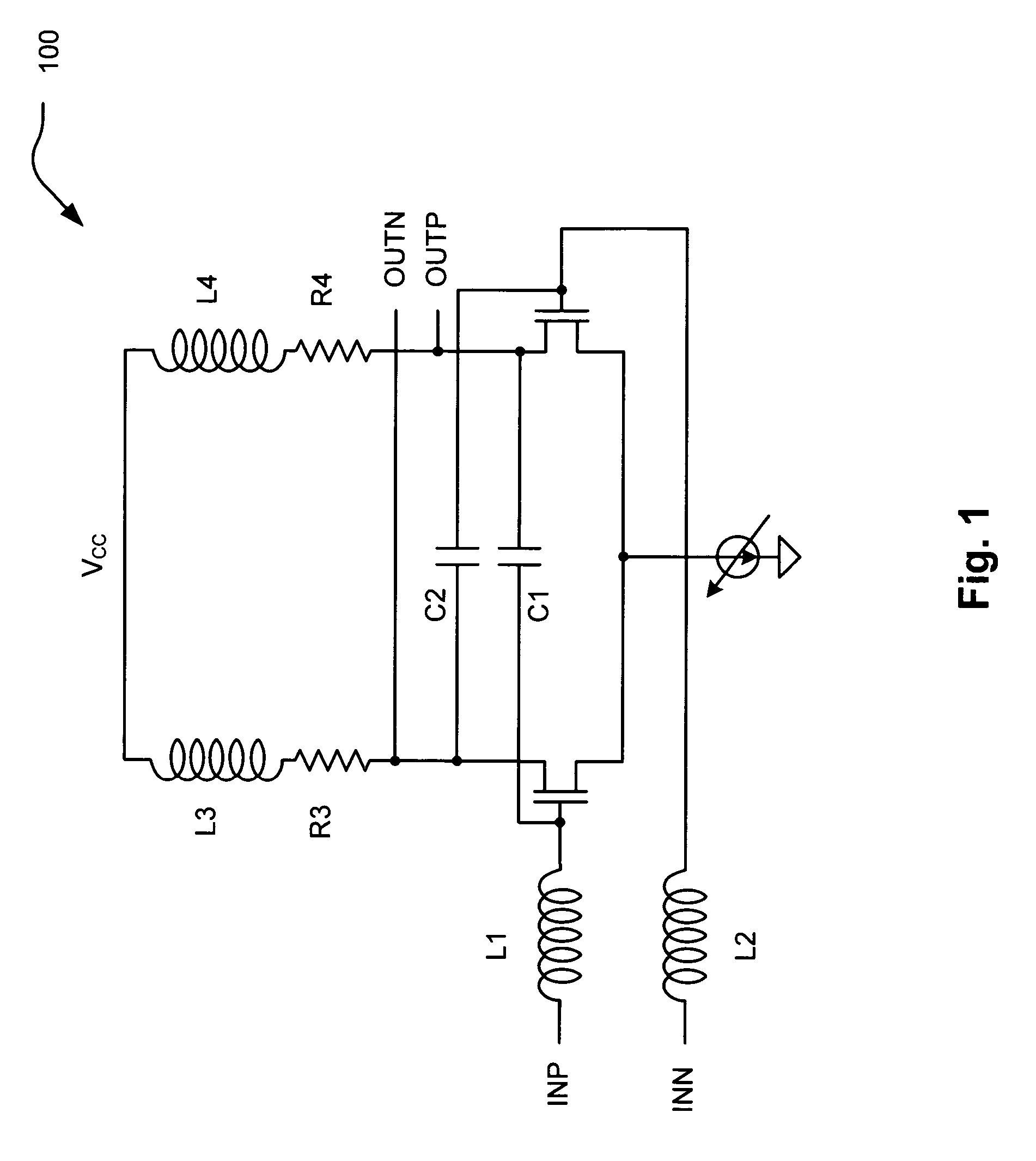
embodiment 100
[0023]FIG. 1 illustrates an embodiment 100 of a current-controlled CMOS (C3MOS) wideband data amplifier circuit. A current source transistor can be biased by a bias voltage so that a constant current flows from drain to source in the current source transistor. Two separate differential transistors compose a wideband differential transistor pair. A first differential transistor has its gate tied to the negative end of a first series peaking inductor L1, while a positive differential input signal INP is coupled to the positive end of the first series peaking inductor L1. Similarly, a second differential transistor has its gate tied to the negative end of a second series peaking inductor L2, while a negative differential input signal INN is coupled to the positive end of the second series peaking inductor L2.
[0024]Assuming that the first and second differential transistors are identical, then the first and second series peaking inductors L1 and L2 have the same inductance. A first outp...
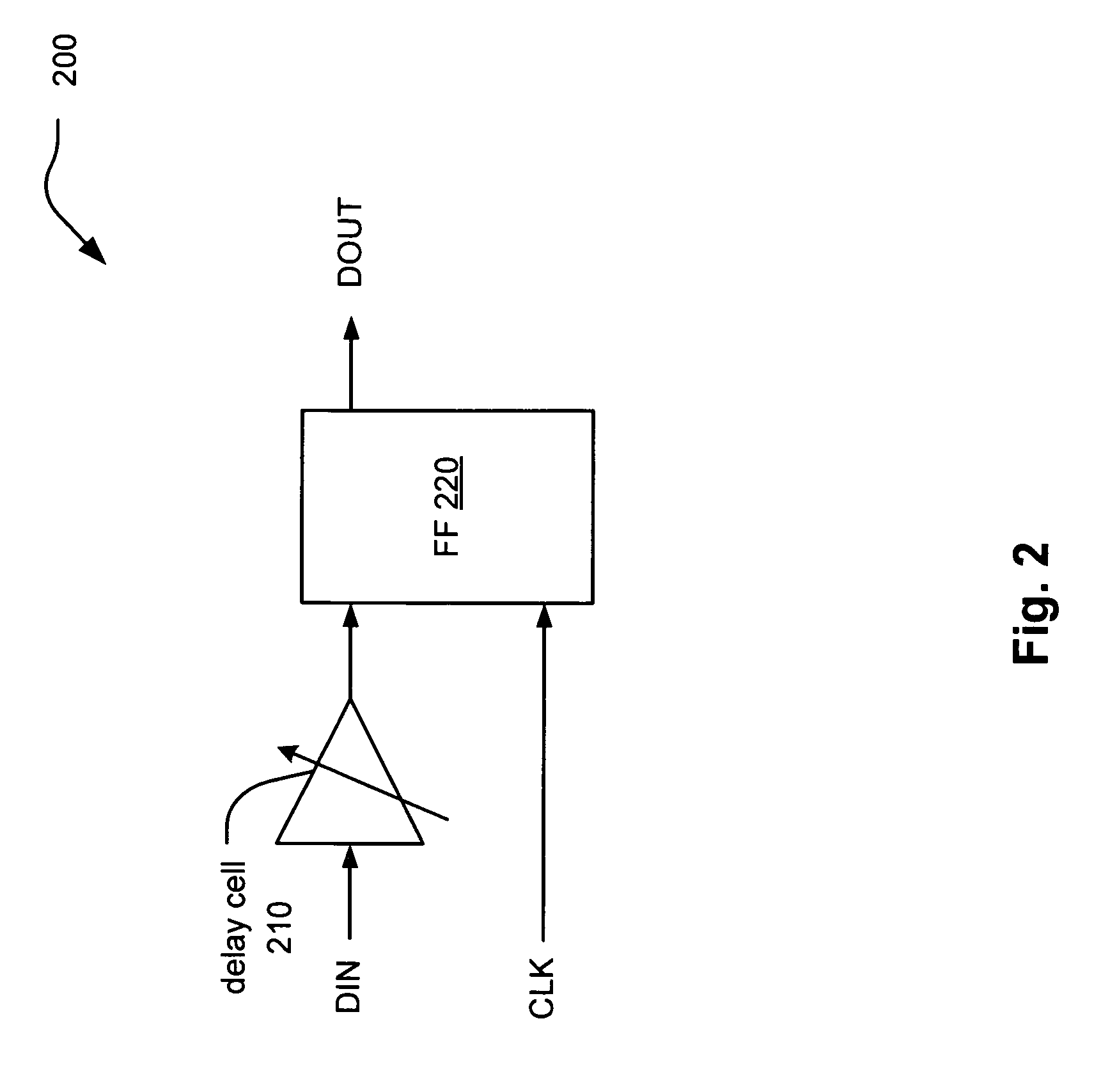
embodiment 200
[0027]FIG. 2 illustrates an embodiment 200 of a variable delay cell. As mentioned above, there is a need in the art for delay cells within many broadband data communication applications. Also, variable delay cells provide for even greater flexibility and applicability than fixed delay type delay cells. This embodiment 200 shows a basic building block of a data synchronization circuit. The input data (DIN) is retimed by a flip-flop (FF) driven by a clock signal (CLK). For the FF to operate correctly, the input data (DIN) and clock (CLK) must satisfy one or more certain timing requirements. A delay cell is often inserted between the input data (DIN) and the FF so that the timing relation between the clock (CLK) and data (DIN) at the input of the FF can be adjusted to compensate for any phase variations of the input signals or circuit delay variations due to changes in process, voltage supply or temperature (PVT). As the input data (DIN) runs at an ever increasing rate, the delay cell ...
embodiment 300
[0029]In the embodiment 300 of a variable delay cell implemented using a 5-tap FIR filter, a goal is to have a data stream with an equal delay (e.g., Δtn) between each of the various components of the data stream. In the embodiment 300, there are 5 components of the data stream. Typically, this delay (e.g., Δtn) is the same, and the delays of each of these delay cells 310, 320, 330, and 340 may be adjusted together.
[0030]Another possible embodiment by which a variable delay cell can be implemented is to add a variable capacitive load at the output of conventional data buffers (e.g., differential pairs). However, there is a fundamental limitation on such an approach. For those circuits whose small-signal transfer function can be approximated by a single-pole response, the bandwidth and delay are directly coupled together. For example, the 10%-90% rise / fall time in response to an input step equals to 0.35 / BW (where BW is the −3 dB bandwidth of the small signal response of the circuit)...
PUM
 Abstract
Description
Claims
Application Information