Light emitting device

a technology of light-emitting devices and light-emitting elements, which is applied in the direction of electroluminescent light sources, organic semiconductor devices, thermoelectric devices, etc., can solve the problems of low light-emitting efficiency and low light-emitting efficiency, and achieve enhanced light-emitting efficiency, low light-emitting efficiency, and enhanced light-emitting efficiency

Active Publication Date: 2009-10-13
SEMICON ENERGY LAB CO LTD
View PDF49 Cites 87 Cited by
  • Summary
  • Abstract
  • Description
  • Claims
  • Application Information

AI Technical Summary

Benefits of technology

[0002]A light-emitting element having a light-emitting layer has been used for a display recently. Such a display using a light-emitting element has advantageous effects such as a wide viewing angle, a high-response speed and low power consumption, as compared with a display having a liquid-crystal layer, and thus, has been developed actively.
[0003]Light-emitting elements have a problem that their light-extraction efficiency is low due to scattered light or reflected light inside the light-emitting elements. The light-extraction efficiency needs to be enhanced.
[0004]In order to enhance the light-extraction efficiency, there is proposed a structure in which a transparent electrode used for an electrode of a light-emitting element has a different thickness according to emission colors (Reference 1: Japanese Patent Laid-Open No. 2003-142277).DISCLOSURE OF INVENTION
[0005]It is an object of the present invention to enhance the light-extraction efficiency of a light-emitting element by a method different from that of Reference 1.
[0006]In order to achieve the object, a thickness of a layer constituting a part of a light-emitting element is made different depending on each emission color, which is one feature of the present invention.
[0007]One mode of the present invention is a light-emitting device comprising a plurality of light-emitting elements. The plurality of light-emitting elements each include a first electrode and a second electrode; and a first layer, a second layer and a third layer which are sequentially formed between the first electrode and the second electrode, wherein the first layer serves as a layer generating holes, the second layer serves as a layer including a light-emitting layer for each emission color, and the third layer serves as a layer generating electrons, and the thickness of the first layer is different depending on each layer including a light-emitting layer.

Problems solved by technology

Light-emitting elements have a problem that their light-extraction efficiency is low due to scattered light or reflected light inside the light-emitting elements.

Method used


Image

  • Light emitting device
  • Light emitting device
  • Light emitting device

Examples


embodiment mode 1

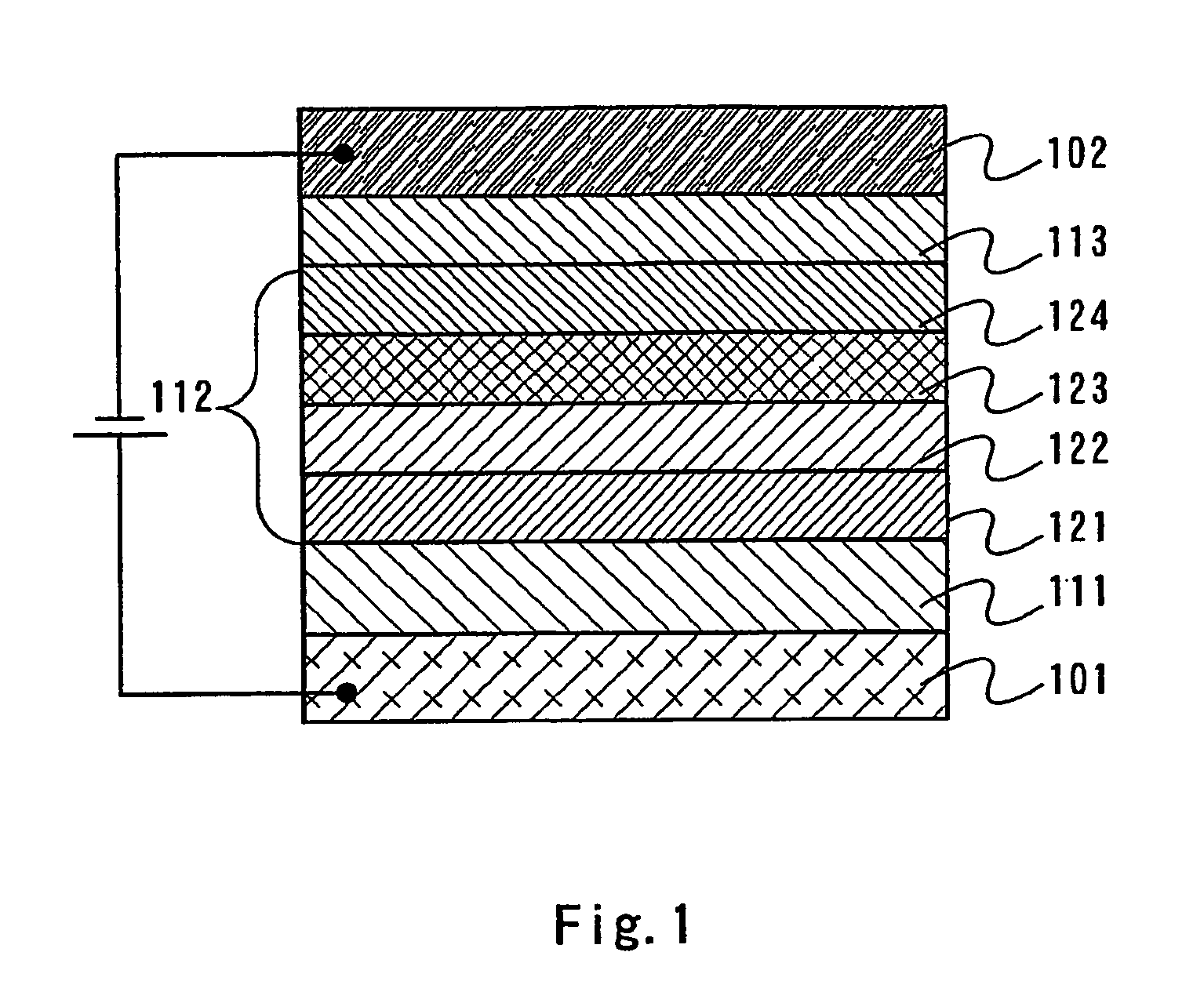
[0043]Embodiment Mode 1 describes a structure of a light-emitting element.

[0044]As shown in FIG. 1, a light-emitting element of the present invention includes a first electrode 101 and a second electrode 102 that are opposed to each other, and a first layer 111, a second layer 112 and a third layer 113 are stacked in this order over the first electrode 101. In such a light-emitting element, holes are injected into the second layer 112 from the first layer 111 and electrons are injected into the second layer 112 from the third layer 113, when a voltage is applied to the light-emitting element such that a potential of the first electrode 101 are higher than that of the second electrode 102. The holes and electrons are recombined in the second layer 112 to excite a light-emitting substance. The excited light-emitting substance emits light when returning to the ground state.

[0045]It is one feature of such light-emitting elements that the thickness of at least one of the layers except th...

embodiment mode 2

[0058]Embodiment Mode 2 describes a structure of a light-emitting element which is different from that of Embodiment Mode 1.

[0059]As shown in FIG. 15, a light-emitting element shown in this embodiment mode includes the first electrode 101 and the second electrode 102 that are opposed to each other, and the first layer 111, the second layer 112, the third layer 113 and a fourth layer 128 that are sequentially stacked over the first electrode 101. One feature of the light-emitting element is to have the fourth layer 128. The fourth layer 128 can be formed with the same material as that of the first layer 111. Other structures are the same as those of Embodiment Mode 1 and thus, the description thereof is omitted.

[0060]When the fourth layer 128 is provided, damages to underlayers in forming the second electrode 102 can be reduced.

[0061]The thickness of the fourth layer 128 is made different depending on each light-emitting element emitting each emission color. Consequently, the decreas...

embodiment mode 3

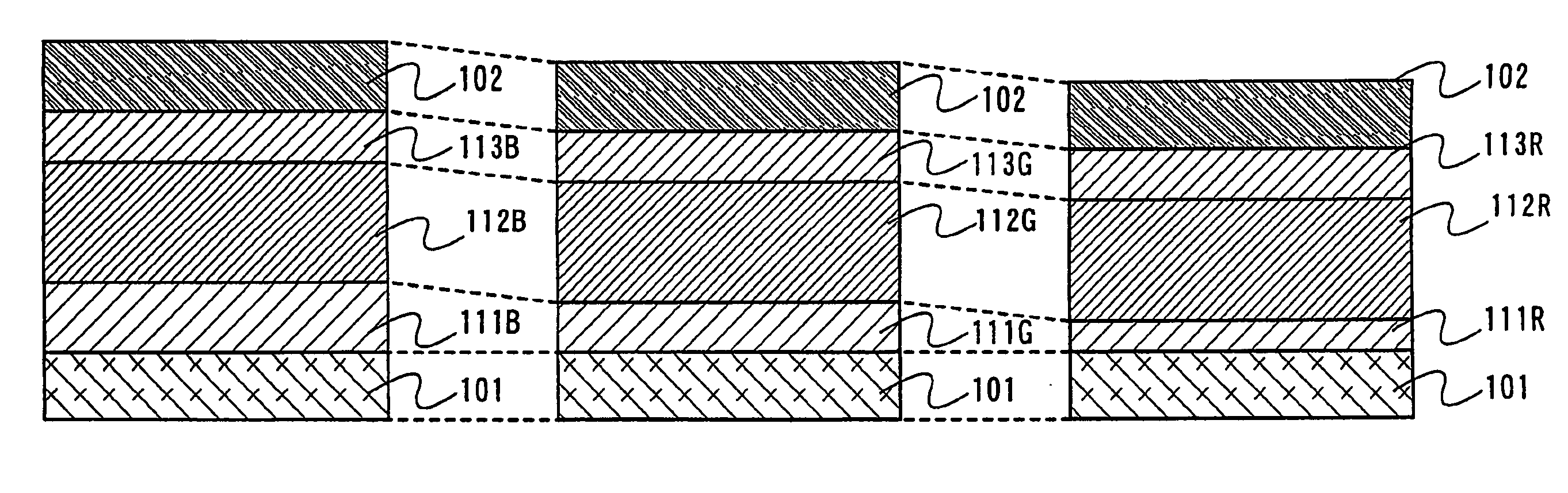
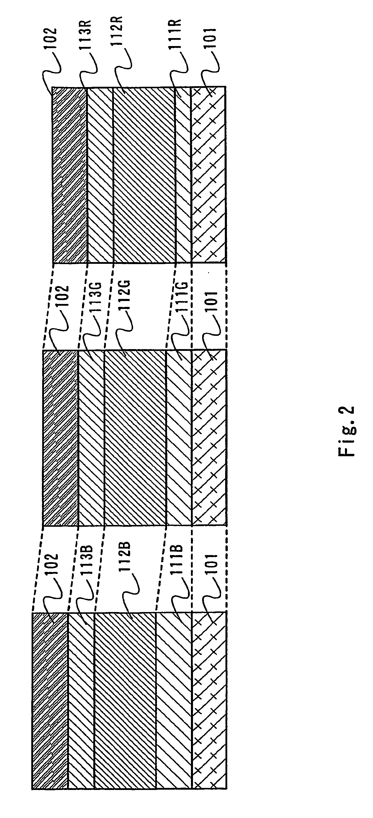
[0065]Embodiment Mode 3 describes a structure in which the thickness of any of layers is made different in a light-emitting device including a color filter.

[0066]As shown in FIG. 16, color filters 115R, 115G and 115B are provided in regions that are to exhibit red (R), green (G) and blue (B) that are different in optical characteristics, respectively. The color filters can be formed using a known material by a screen printing method, a droplet discharging method or the like. FIG. 16 shows the case where the color filters 105R, 105G and 105B are provided on the second electrode side 102 (on the emission side), and in this case, the second electrode 102 needs to be light-transmitting.

[0067]The structure of the light-emitting element is as follows: the first layers H1R, H1G and H1B, the second layers 112R, 112G, and 112B, the third layers 113R, 113G and 113B, and the second electrode 102 are formed sequentially over the first electrode 101. Since each color is generated by the color fi...


PUM


Abstract

Light-emitting elements have a problem that their light-extraction efficiency is low due to scattered light or reflected light inside the light-emitting elements. The light-extraction efficiency of the light-emitting elements needs to be enhanced by a new method. According to the present invention, a light-emitting element includes a first layer generating holes, a second layer including a light-emitting layer for each emission color and a third layer generating electrons between an anode and a cathode, and the thickness of the first layer is different depending on each layer including the light-emitting layer for each emission color. A layer in which an organic compound and a metal oxide are mixed is used as the first layer, and thus, the driving voltage is not increased even when the thickness is increased, which is preferable.

Description

TECHNICAL FIELD[0001]The present invention relates to a light-emitting element having a light-emitting layer, a light-emitting device having the light-emitting element, and a manufacturing method thereofBACKGROUND ART[0002]A light-emitting element having a light-emitting layer has been used for a display recently. Such a display using a light-emitting element has advantageous effects such as a wide viewing angle, a high-response speed and low power consumption, as compared with a display having a liquid-crystal layer, and thus, has been developed actively.[0003]Light-emitting elements have a problem that their light-extraction efficiency is low due to scattered light or reflected light inside the light-emitting elements. The light-extraction efficiency needs to be enhanced.[0004]In order to enhance the light-extraction efficiency, there is proposed a structure in which a transparent electrode used for an electrode of a light-emitting element has a different thickness according to em...

Claims


Application Information

Patent Timeline
Patent Type & Authority Patents(United States)
IPC IPC(8): H01L35/24G02B5/20H01L51/50H05B33/12H05B33/14H05B33/24H05B33/26H05B33/28H05B44/00
CPCH01L27/156H01L51/5088H01L27/322H01L27/3244H01L51/0059H01L51/0071H01L2251/5315H01L2251/558H01L51/0081Y02E10/549H10K59/38H10K59/12H10K85/631H10K85/657H10K85/324H10K50/17H10K2102/3026H10K2102/351H10K30/82H05B33/145
Inventor SEO, SATOSHIKUMAKI, DAISUKEIKEDA, HISAOSAKATA, JUNICHIRO
Owner SEMICON ENERGY LAB CO LTD
Why Eureka
Try Eureka