Laser repairing method of electroluminescent display device

a technology of electroluminescent display device and laser repair method, which is applied in the manufacture of electrode systems, electric discharge tubes/lamps, instruments, etc., can solve the problems of dark spot display defect, damage to cathode layer b>5/b>, etc., and achieve high resistivity region

Active Publication Date: 2009-11-03
SANYO ELECTRIC CO LTD
View PDF18 Cites 26 Cited by
  • Summary
  • Abstract
  • Description
  • Claims
  • Application Information

AI Technical Summary

Benefits of technology

[0009]The invention provides a method of repairing an electroluminescent display panel using laser. The method includes providing a panel to be assembled into an electroluminescent display device. The panel includes a plurality of pixels each including an electroluminescent element having an electroluminescent layer formed between an anode layer

Problems solved by technology

However, when the laser beams are not properly radiated to the foreign substance 6, the cathode layer 5 is damaged by the energy of the laser beams and can be torn to form a pin

Method used


Image

  • Laser repairing method of electroluminescent display device
  • Laser repairing method of electroluminescent display device
  • Laser repairing method of electroluminescent display device

Examples


Embodiment Construction

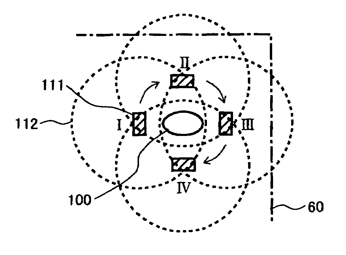
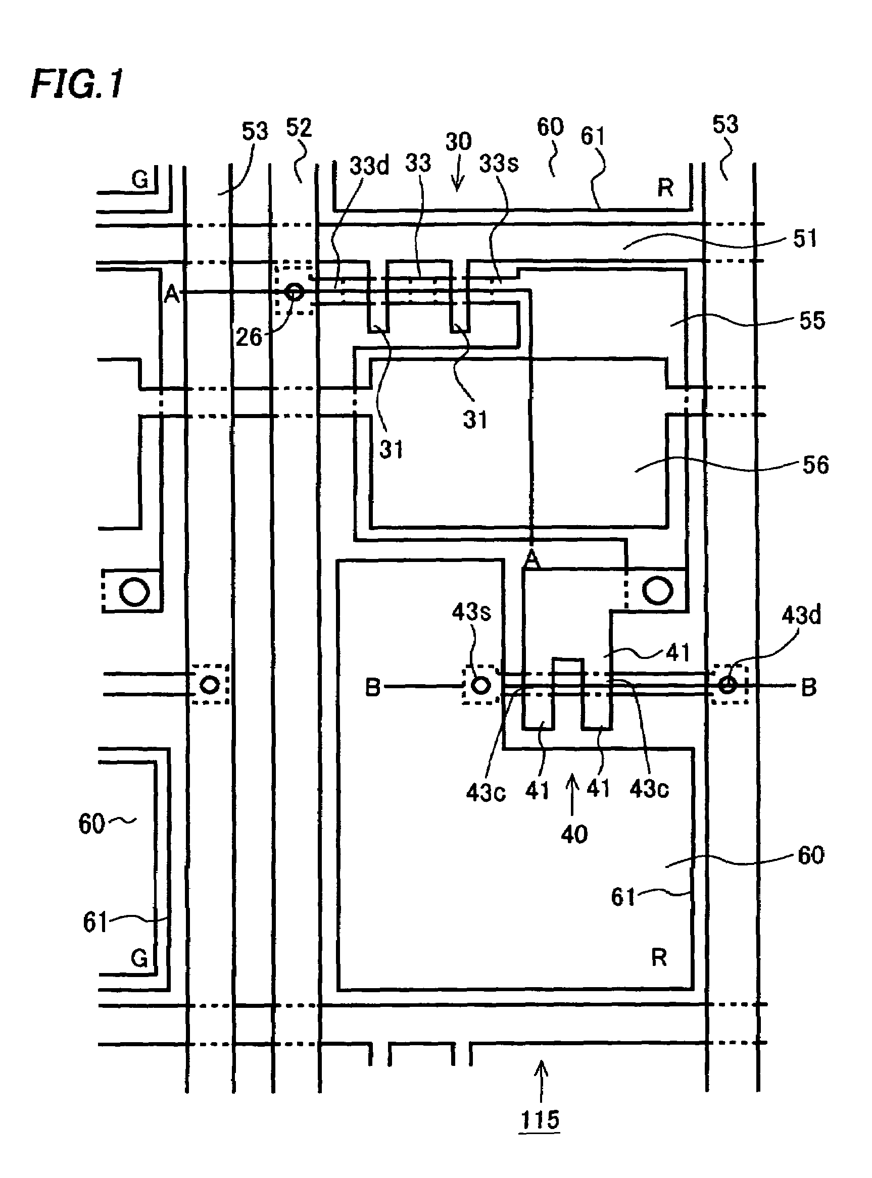
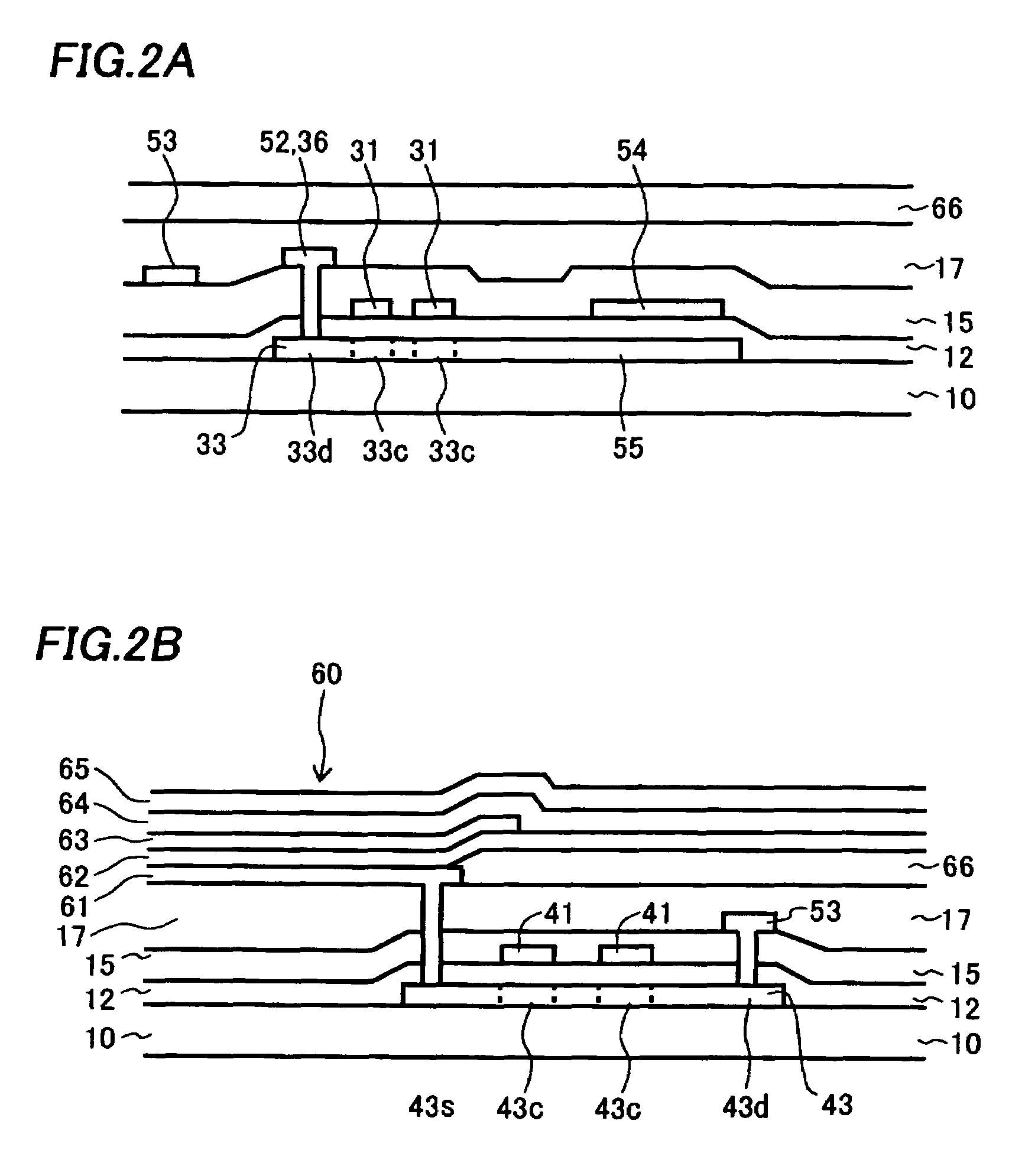
[0016]An embodiment of the invention will be described with reference to the drawings in detail. An organic EL display device of this embodiment will be described first. FIG. 1 is a plan view showing a pixel of the organic EL display device. FIG. 2A is a cross-sectional view along line A-A of FIG. 1, and FIG. 2B is a cross-sectional view along line B-B of FIG. 1.

[0017]As shown in FIGS. 1, 2A, and 2B, a pixel 115 is formed in a region enclosed with a gate signal line 51 and a drain signal line 52. A plurality of the pixels 115 is arranged in a matrix configuration.

[0018]An organic EL element 60 as a self-emissive element, a switching TFT (thin film transistor) 30 for controlling a timing of supplying an electric current to the organic EL element 60, an organic EL element driving TFT 40 for supplying an electric current to the organic EL element 60, and a storage capacitor 56 are disposed in the pixel 115.

[0019]The switching TFT 30 is provided on a periphery of the intersection of the...


PUM


Abstract

The invention is directed to repairing of a defective portion caused by a short circuit without generating a dark spot by a pin hole. Laser beams are irradiated to an irradiating region set in a peripheral region of a foreign substance. This prevents damaging of an organic EL element which the foreign substance adheres to and formation of the pin hole. By irradiating laser beams to the peripheral region at a distance from the foreign substance, energy of the laser beams spreads concentrically around the irradiating region, and is also supplied to the foreign substance indirectly. Therefore, the high resistive region can be formed between an anode layer and a cathode layer so that the defective portion caused by the short circuit by the foreign substance can be repaired.

Description

BACKGROUND OF THE INVENTION[0001]1. Field of the Invention[0002]The invention relates to a laser repairing method of an electroluminescent display device having a plurality of pixels and an electroluminescent element provided in each of the pixels and formed by interposing an electroluminescent layer between an anode layer and a cathode layer.[0003]2. Description of the Related Art[0004]An organic electroluminescent (hereafter, referred to as EL) display device using organic EL elements is receiving an attention as a new display device substituted for a CRT or an LCD.[0005]FIG. 5 is a cross-sectional view showing a structure of such an organic EL element. An anode layer 1 made of ITO (indium tin oxide) is formed on a transparent insulating substrate 10 such as a glass substrate, and an organic EL layer formed of a hole transport layer 2, an emissive layer 3, and an electron transport layer 4 is laminated thereon. A cathode layer 5 is formed on this organic EL layer. A potential diff...

Claims


Application Information

Patent Timeline
IPC IPC(8): B05D5/06B05D3/00B32B43/00C08J7/18H01J9/50H05B33/10G09G3/00H01L27/32H01L51/50H01L51/56
CPCG09G3/006H01L2251/568H01L51/56H10K71/861H10K71/00H05B33/10
Inventor NISHIKAWA, RYUJINAGATA, RYOZOOGAWA, TAKASHI
Owner SANYO ELECTRIC CO LTD
Why Eureka
Try Eureka