Semiconductor integrated circuit, and designing method and testing method thereof

a technology of semiconductor integrated circuit and design method, applied in the direction of electronic circuit testing, measurement devices, instruments, etc., can solve the problems of increasing the difficulty of testing semiconductor integrated circuits, increasing the scale and complexity of semiconductor integrated circuits, and increasing the frequency of operation failures

Inactive Publication Date: 2009-11-03
PANASONIC CORP
View PDF10 Cites 26 Cited by
  • Summary
  • Abstract
  • Description
  • Claims
  • Application Information

AI Technical Summary

Benefits of technology

[0025]An object of the present invention is to provide a semiconductor integrated circuit which can be tested using a clock signal having a high frequency without a high-performance tester, by utilizing an oscillator circuit provided inside the semiconductor integrated circuit, even when the semiconductor integrated circuit has a clock stop control circuit for controlling output of a clock signal, and a designing method and a testing method thereof.
[0027]Thereby, a last pulse of a clock signal used when a scan path circuit performs a capture operation is caused not to fall and is held in a state in which a value there of is fixed, so that a clock pulse can be caused to fall after a scan enable signal reaches each circuit section. Therefore, even when a semiconductor integrated circuit has a clock stop control circuit for controlling a clock signal, the clock stop control circuit can reliably output a clock signal which is used by a scan path circuit to perform a shift-out operation. Therefore, when a capture operation is performed, a clock signal having an actual operating speed generated in a semiconductor integrated circuit can be used, so that delay testing or the like can be performed without using a high-speed tester.
[0045]Thereby, a clock signal having an actual operating speed generated in a semiconductor integrated circuit can be used, thereby making it possible to perform delay testing or the like without using a high-speed tester.
[0049]According to the present invention, even when a semiconductor integrated circuit has a clock stop control circuit for controlling a clock signal, a clock signal having an actual operating speed required for delay testing, which is generated in the semiconductor integrated circuit, can be used, thereby making it possible to perform a test, such as delay testing, BIST, or the like, without using a high-speed tester.

Problems solved by technology

In recent years, the scale and complexity of semiconductor integrated circuits are rapidly increased with rapid progress in technology for nanometer semiconductor manufacturing process.
Due to this, it is increasingly difficult to test semiconductor integrated circuits.
However, when a clock signal having a high frequency is used during an actual operation, an operational failure increasingly often occurs in a semiconductor integrated circuit with advances in nanometer technology for semiconductor integrated circuits.
This is because, for example, a small defect is likely to emerge in nanometer semiconductor elements and wirings; a variation in quality occurring due to a variation in each manufacturing process of semiconductor integrated circuits becomes obvious when a clock signal having a high frequency is used; manufacturing steps are complicated; and the like.
However, the conventional scan test is insufficient to test such an operational failure depending on the clock frequency.
However, as the speed of semiconductor integrated circuits is increased, it is becoming considerably difficult to externally supply a test pulse having the same frequency as that used during an actual operation.
However, actually, the high-speed tester which can supply a clock signal having a frequency of 1 GHz is considerably expensive, leading to an increase in cost.
Therefore, when the delay is large, or a clock frequency during a test is high, it may be difficult to avoid the deviation.
Therefore, in semiconductor integrated circuits having a gated clock circuit as illustrated in FIG. 4, it is not possible in the conventional art to perform a scan test in which an externally supplied clock signal is used for a test during the shift operation, and a clock output by a clock generating circuit on a semiconductor integrated circuit is used during the capture operation.

Method used


Image

  • Semiconductor integrated circuit, and designing method and testing method thereof
  • Semiconductor integrated circuit, and designing method and testing method thereof
  • Semiconductor integrated circuit, and designing method and testing method thereof

Examples


first embodiment

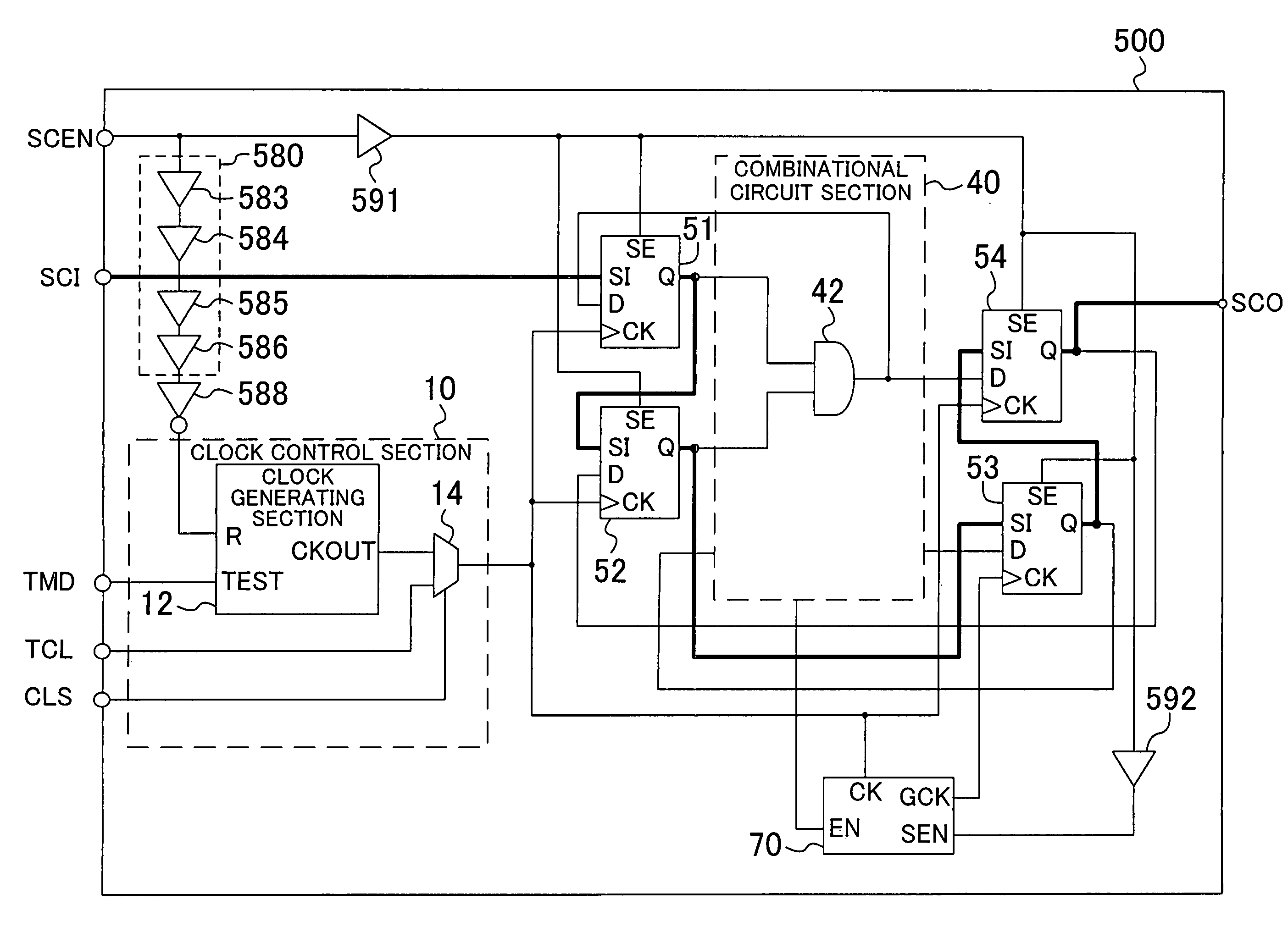
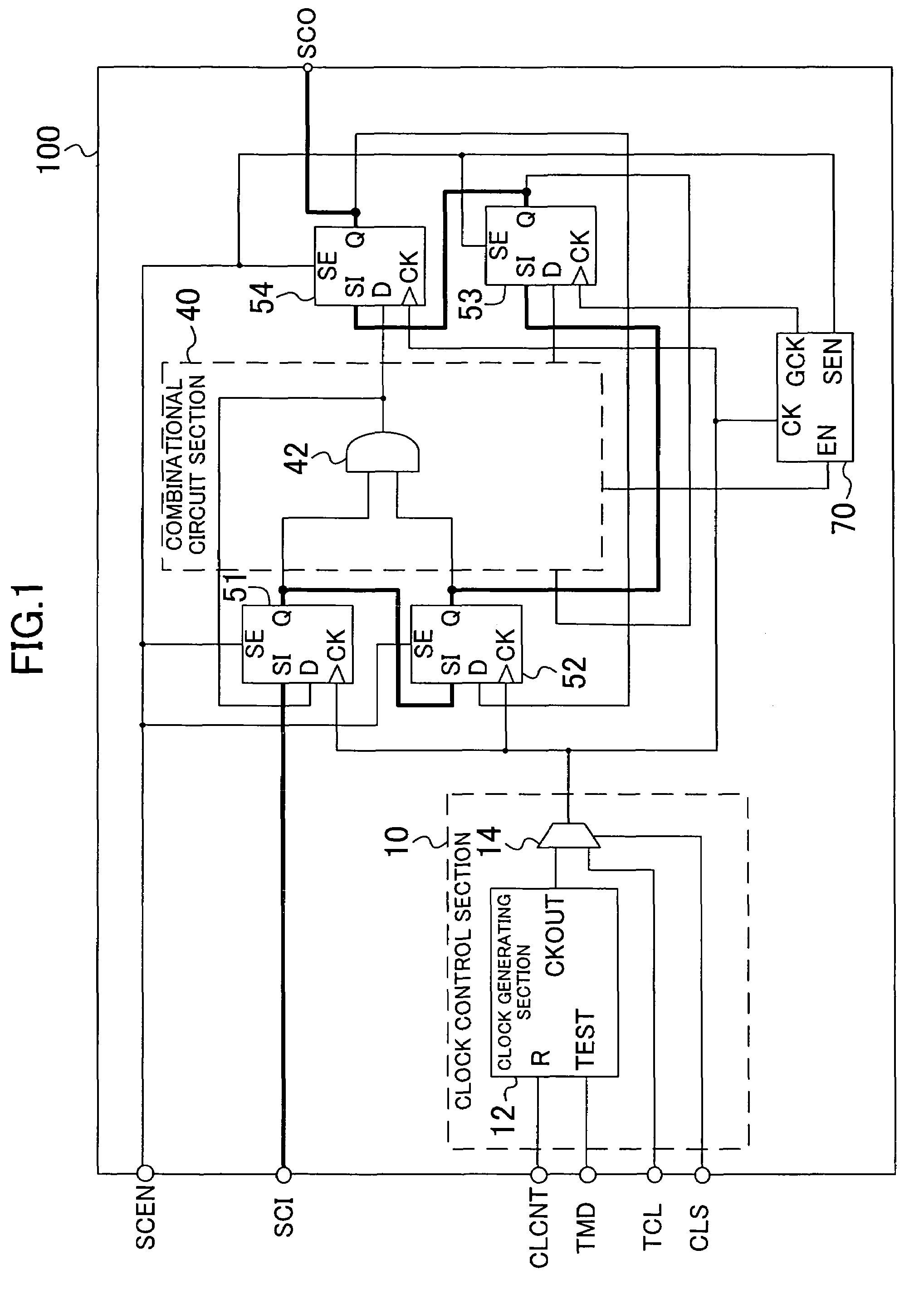
[0077]FIG. 1 is a block diagram illustrating a semiconductor integrated circuit according to a first embodiment of the present invention. The semiconductor integrated circuit 100 of FIG. 1 comprises a clock control section 10, a combinational circuit section 40, scan flip-flops 51, 52, 53 and 54, and a gated clock circuit 70 as a clock stop control circuit. The clock control section 10 comprises a clock generating section 12, and a selector 14 as a selection section. The combinational circuit section 40 comprises an AND gate 42. The scan flip-flops 51 to 54 constitute a scan path circuit.

[0078]The gated clock circuit 70 controls supply of a clock to the scan flip-flop 53. A scan-in terminal SCI, the scan flip-flop 51, the scan flip-flop 52, the scan flip-flop 53, the scan flip-flop 54, and the scan-out terminal SCO are connected together so as to transfer data in this order, constituting a scan chain. The combinational circuit section 40 is operated, depending on changes in output s...

second embodiment

[0109]FIG. 7 is a block diagram illustrating a semiconductor integrated circuit according to a second embodiment of the present invention. The semiconductor integrated circuit 200 of FIG. 7 is the same as the semiconductor integrated circuit 100 of FIG. 1, except that a clock control section 210 is provided instead of the clock control section 10. The clock control section 210 comprises a clock generating section 212 and a selector 14. Parts other than the clock generating section 212 are similar to those of the first embodiment and are indicated with the same reference numerals, and will not be described.

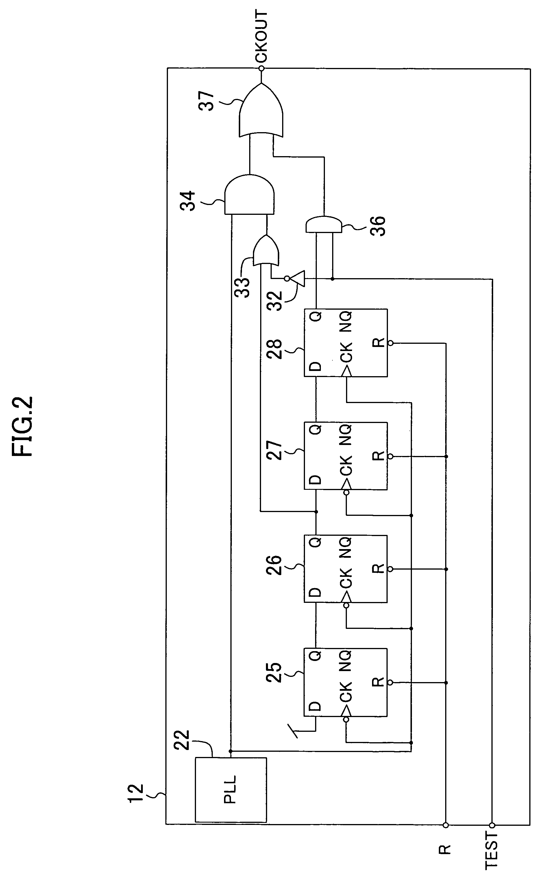
[0110]FIG. 8 is a circuit diagram illustrating an exemplary configuration of the clock generating section 212 of FIG. 7. The clock generating section 212 is the same as the clock generating section 12 of FIG. 2, except that a counter circuit section 224 as a period control circuit is provided instead of the flip-flops 25 and 26.

[0111]FIG. 9 is a circuit diagram illustrating an exem...

third embodiment

[0119]FIG. 10 is a block diagram illustrating a semiconductor integrated circuit according to a third embodiment of the present invention. The semiconductor integrated circuit 300 of FIG. 10 is the same as the semiconductor integrated circuit 100 of FIG. 1, except that a clock control section 310 is provided instead of the clock control section 10. The clock control section 310 comprises a clock generating section 312 and a selector 14. A test clock signal input to the test clock terminal TCL is also input to the clock generating section 312. Parts other than the clock generating section 312 are similar to those of the first embodiment and are indicated with the same reference numerals, and will not be described.

[0120]FIG. 11 is a circuit diagram illustrating an exemplary configuration of the clock generating section 312 of FIG. 10. The clock generating section 312 is the same as the clock generating section 12 of FIG. 2, except that a flip-flop 329 is further provided. An output of...


PUM


Abstract

A semiconductor integrated circuit comprises a combinational circuit section having a combinational circuit, a scan path circuit for inputting and outputting a value from and to the combinational circuit section in accordance with a scan enable signal and in synchronization with a clock signal, and a clock control section for generating and outputting a predetermined number of pulses as the clock signal after a predetermined period has passed since a time when an output command signal was received. The clock control section has an oscillator circuit for generating and outputting the pulse, and is configured to output a last pulse of the predetermined number of pulses in a manner which holds a logical value immediately after an active edge for the scan path circuit.

Description

BACKGROUND OF THE INVENTION[0001]The present invention relates to a semiconductor integrated circuit, and a designing method and a testing method thereof, and more particularly, to a technique for improving the quality of a test.[0002]In recent years, the scale and complexity of semiconductor integrated circuits are rapidly increased with rapid progress in technology for nanometer semiconductor manufacturing process. Due to this, it is increasingly difficult to test semiconductor integrated circuits. To address this problem, a designing method which employs a scan test, a Built-in Self Test (BIST), or the like has been developed as a means for facilitating a test of a semiconductor integrated circuit. Since such a method has been widespread, faults represented by the stuck-at fault model can be efficiently tested. When faults represented by the stuck-at fault model are detected, the capability to detect the fault does not depend on the clock frequency. Therefore, when a conventional...

Claims


Application Information

Patent Timeline
Patent Type & Authority Patents(United States)
IPC IPC(8): G01R31/28
CPCG01R31/318552
Inventor TAKEOKA, SADAMIYOSHIMURA, SHINICHI
Owner PANASONIC CORP
Why Eureka
Try Eureka