Adder and current mode switching regulator

a current mode switching and regulator technology, applied in the direction of process and machine control, instruments, computation using denominational number representation, etc., can solve the problems of complex manufacturing process and inability to reduce chip size, and achieve the effect of simplifying the process of current mode switching regulator semiconductor devices, reducing manufacturing costs and reducing chip siz

Inactive Publication Date: 2009-11-10
ABLIC INC
View PDF2 Cites 22 Cited by
  • Summary
  • Abstract
  • Description
  • Claims
  • Application Information

AI Technical Summary

Benefits of technology

[0024]With the structure described above, according to the present invention, in the case where the added results that are output by the respective transistors that constitute the prestage VI converter, the poststage VI converter, the first current mirror circuit, and the second current mirror circuit in the first VI converter and the second VI converter are varied due to a variation in the threshold voltage in the process, the amount of current is adjusted, thereby making it possible to suppress a variation caused by the threshold voltage in the adjustment resistor and / or the adjustable second current mirror circuit. As a result, all of the transistors can be formed with the CMOS structure instead of structuring the transistors by the bipolar transistors or the bi CMOS transistors as in the conventional art. Also, the process of the current mode switching regulator semiconductor device is simplified, the chip size can be reduced, and the manufacturing costs can be reduced.
[0025]As a result, according to the present invention, by using the above-mentioned adder, there can be inexpensively structured the current mode switching regulator which is capable of adding the sense voltage corresponding to the current that flows in the coil and the voltage of the compensation lamp waveform together without any variation between the chips, and outputting the output voltage corresponding to the load at a high speed and with a high precision.

Problems solved by technology

However, in the case where the respective circuits including the adder 103 are formed of the bipolar transistor or the bi CMOS transistor, there is a disadvantage in that a manufacturing process gets complicated as compared with the CMOS, and miniaturization cannot be conducted with the result that the chip size cannot be reduced.

Method used


Image

  • Adder and current mode switching regulator
  • Adder and current mode switching regulator
  • Adder and current mode switching regulator

Examples


Embodiment Construction

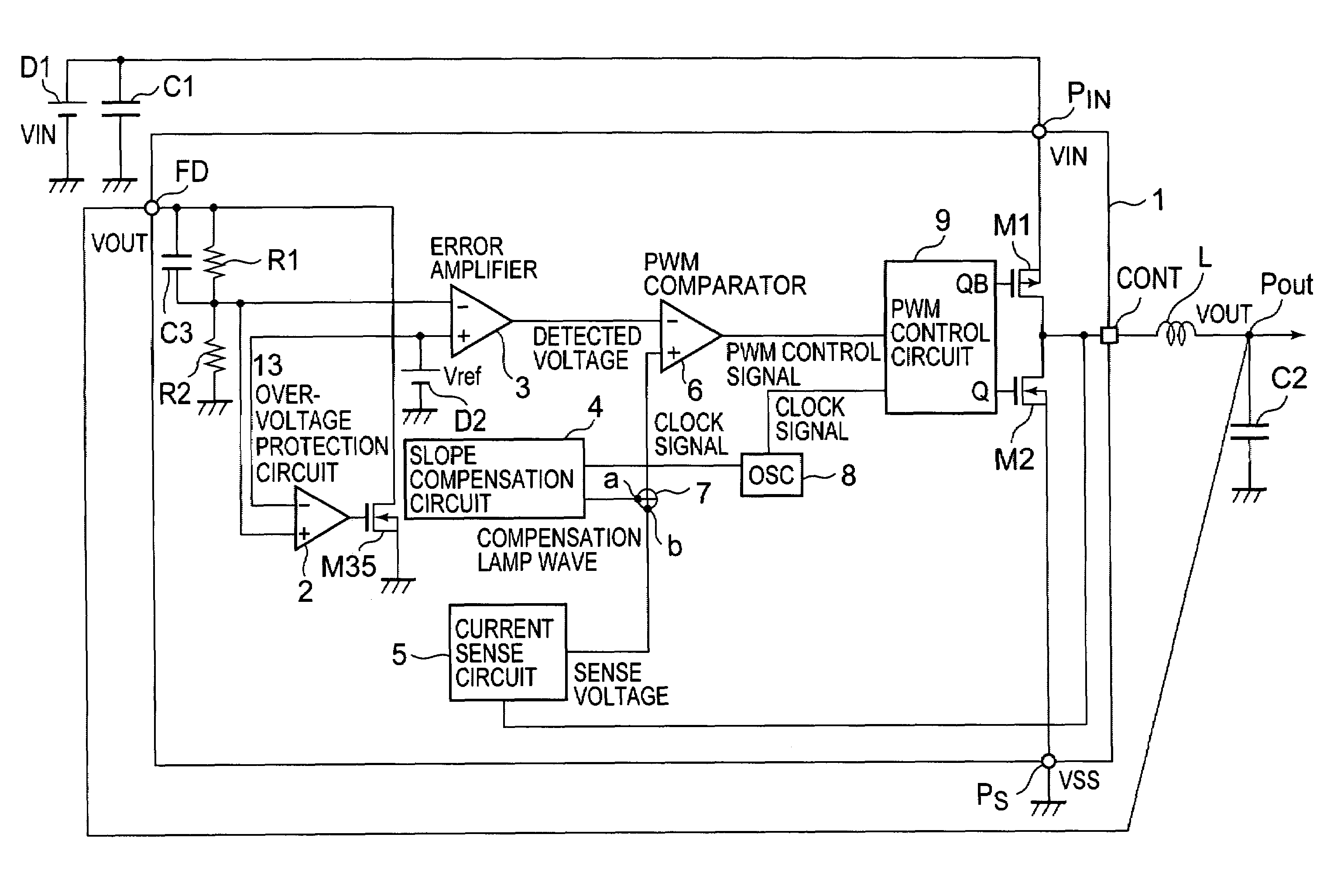
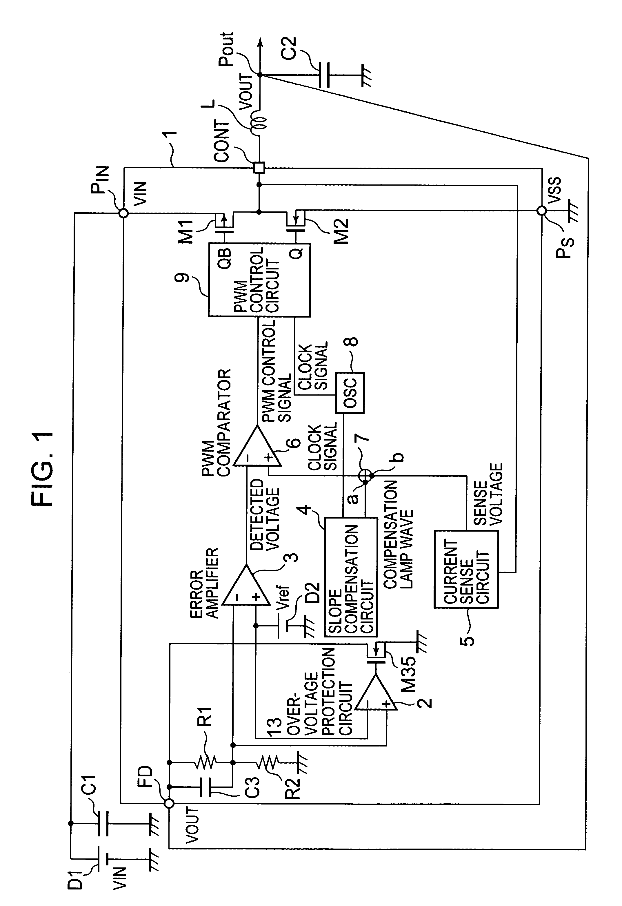
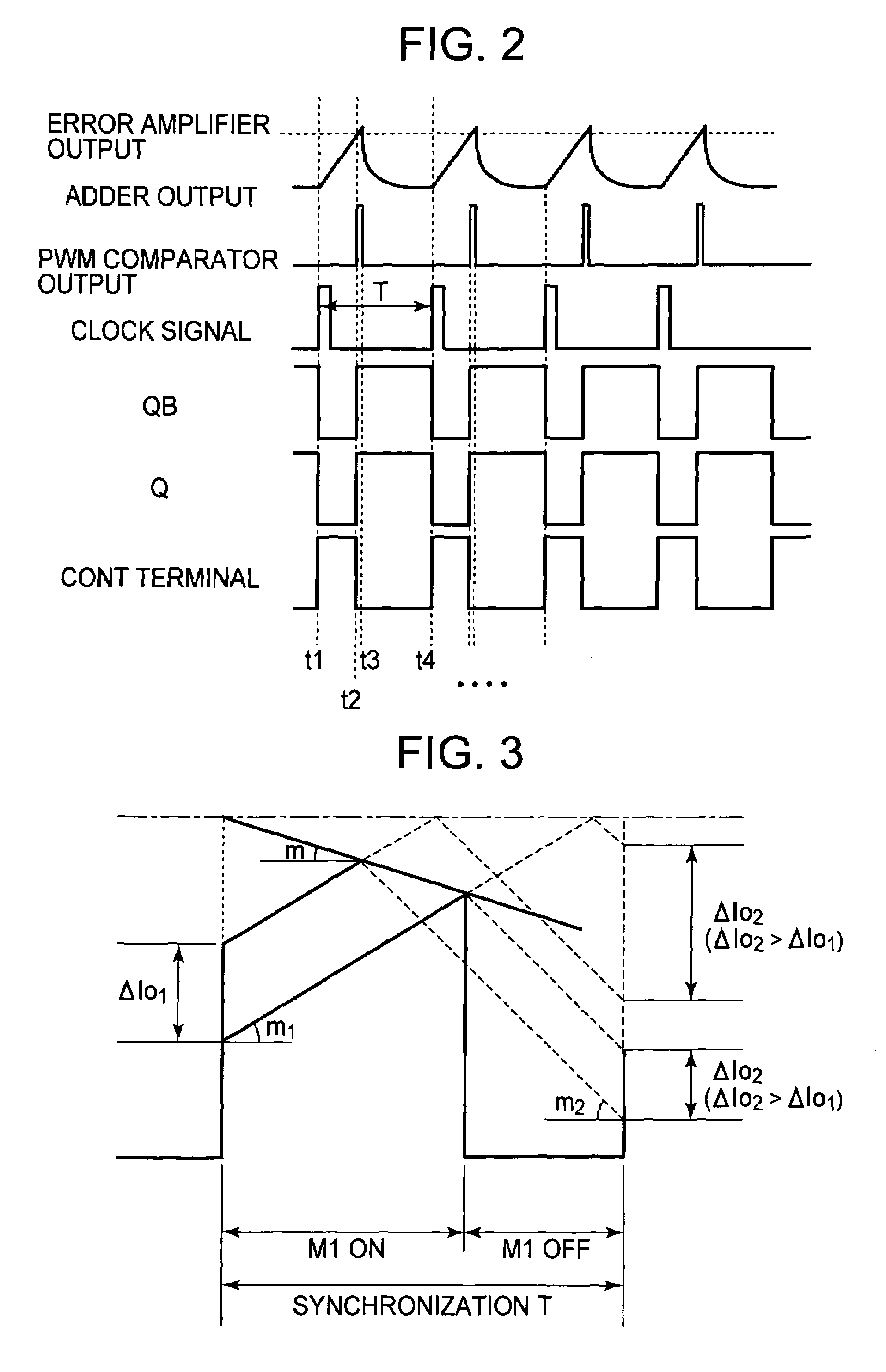
[0034]Hereinafter, a description will be given of a current mode step-down switching regulator semiconductor device 1 using a current sense circuit 5 according to a embodiment of the present invention with reference to the accompanying drawings. FIG. 1 is a block diagram showing a structure example of the current mode step-down switching regulator according to the embodiment of the present invention. The most characteristic structure of the present invention resides in an adder 7 that adds the voltage of the compensation lamp wave and the sense voltage that is output by the current sense circuit 5 in order to generate a voltage that controls the output voltage Vout which is output from the output terminal Pout, and its details will be described.

[0035]In the figure, the current mode step-down switching regulator according to this embodiment is made up of a current mode step-down switching regulator semiconductor device 1, a coil L used for voltage conversion (step-down in this embodi...


PUM


Abstract

Provided is an adder in which all of circuits can be constituted by CMOS transistors, a process is simplified, and a chip size can be reduced as compared with a conventional art. The adder according to the present invention includes: a first VI converter and a second VI converter that allow a current corresponding to an input voltage to flow therein; and a current addition resistor having one end commonly connected to output terminals of the first VI converter and the second VI converter and another end grounded, which is adjustable in a resistance value. Each of the first VI converter and the second VI converter includes: a prestage VI converter that generates a reference current; a poststage VI converter that generates a current corresponding to the input voltage; a first current mirror circuit whose first terminal on a reference side is connected with the prestage VI converter and whose first output terminal in which a current corresponding to the first terminal flows is connected with the poststage VI converter; and a second current mirror circuit whose second terminal on the reference side is connected to the first output terminal, and which can adjust a current ratio from a second output terminal in correspondence with the current that flows in the second terminal. A voltage at the one end of the current addition resistor is output as an addition voltage.

Description

BACKGROUND OF THE INVENTION[0001]1. Field of the Invention[0002]The present invention relates to a current mode switching regulator that controls an output voltage on the basis of the detected values of the output voltage and an output current by the aid of a DC input power supply, and an adder used for the switching regulator.[0003]2. Description of the Related Art[0004]A circuit structured as shown in FIG. 6 is used for a current mode step-down switching regulator (for example, refer to JP 2002-281742 A).[0005]In the circuit, when a switch 107 is turned on, a current flows into a coil 108 from a power supply with the result that an input voltage Vi is accumulated in the coil 108 as an electric energy (that is, electric charges), and also accumulated in an output capacitor 112. Also, when the switch 107 is turned off, the electric energy that has been accumulated in the output capacitor 112 is discharged through a load.[0006]Accordingly, in the current mode step-down switching regu...

Claims


Application Information

Patent Timeline
Patent Type & Authority Patents(United States)
IPC IPC(8): G05F3/16G06F7/42
CPCG06G7/14H02M3/156H02M2001/0025H02M1/0025G05F3/24
Inventor UEHARA, OSAMU
Owner ABLIC INC
Why Eureka
Try Eureka