
Spread spectrum clock generator

a clock generator and spectrum technology, applied in the direction of generating/distributing signals, instruments, wireless commuication services, etc., can solve the problems of circuits that supply clocks, circuits that cannot achieve desired modulation, and increase the frequency of clocks, so as to prevent the effect of reducing the effect of emi reduction and reducing the component used for emi measures

Active Publication Date: 2009-11-17
RENESAS ELECTRONICS CORP
View PDF9 Cites 9 Cited by
  • Summary
  • Abstract
  • Description
  • Claims
  • Application Information

AI Technical Summary

Benefits of technology

[0019]As described before, when the characteristics of the filter and the VCO have varied and then a frequency response speed is slow, a target frequency is switched before the frequency of the modulated clock becomes the target frequency, as shown in FIG. 12. The degree of frequency modulation is thus reduced. The larger the degree of the modulation, the larger the effect of reducing the EMI tends to be. Thus, in the case of FIG. 12, the degree of the modulation becomes smaller than is expected, so that the effect of reducing the EMI is reduced.
[0020]On the contrary, when the frequency response speed is fast, there are generated states in which the frequency of the modulated clock exceeds the target frequency and states in which the frequency of the modulated clock is stabilized at the target frequency. When a clock that exceeds the operating frequency of the circuit that supplies the clock is fed, a malfunction may be caused. On the other hand, when the frequency remains unchanged, the effect of spectrum spreading will be reduced, so that the effect of reducing the EMI may decrease.
[0064]According to the present invention, reduction in an EMI reduction effect can be prevented.
[0065]According to the present invention, the modulation degree is made to be a desired value (a constant value) irrespective of the manufacturing variations or an environment used. A malfunction of a circuit for supplying a clock can be thereby prevented.
[0067]According to the present invention, a component used for EMI measures can be reduced.

Problems solved by technology

In conventional configurations described above, there is a problem that a desired degree of modulation cannot be obtained due to the following reasons:manufacturing variations in the semiconductor integrated circuit; anda use environment such as a supply voltage, ambient temperature, and a frequency used.
On the contrary, when the degree of modulation is great, the maximum frequency of the clock will be increased, so that the circuit which supplies the clock may malfunction.

Method used


Image

  • Spread spectrum clock generator
  • Spread spectrum clock generator
  • Spread spectrum clock generator

Examples


third embodiment

[0120]As the present invention, by repeating transition of the modulation control signal α only in a negative direction, such as 0, −1, . . . , −(A−1), −A, −(A−1), . . . −1, 0, −1 . . . , and the like, modulation of a up-spread type to a high frequency can be implemented.

[0121]Further, the transition of the modulation control signal α should be just in the range of the maximum value A. The pattern of the transition is not limited to those described above. Accommodation to various systems thereby becomes readily possible.

[0122]FIG. 7 is a diagram showing a configuration of a fourth embodiment of the present invention. Referring to FIG. 7, a third program counter 111 is provided in a stage subsequent to the second delay control type oscillator 108 in the first embodiment in FIG. 1. The third programmable counter 111 frequency divides the output of the second delay control type oscillator 108 by L. In the frequency division by L, the period which provides a basis for the frequency divi...

fourth embodiment

[0123]In the present invention, the frequency band of an output modulated clock can be expanded without expanding the frequency bands of the delay control type oscillators. Thus, an increase in the area is small because a low frequency band is handled.

[0124]Next, other embodiment of the present invention will be described. FIG. 8 is a diagram showing a configuration of a fifth embodiment of the present invention. The fifth embodiment of the present invention shows a case where the invention has been applied to a delay-type phase adjustment circuit (DLL: Delay Locked Loop).

[0125]In the delay-type phase adjustment circuit, a phase comparator 202 and a delay control circuit 203 perform an adjustment operation so that the delay value of a first variable delay circuit 201 becomes the length of one period of a received clock signal RCLK.

[0126]A second variable delay circuit 205 has the same characteristics as the first variable delay circuit 201. In order to output a desired phase set by ...

first embodiment

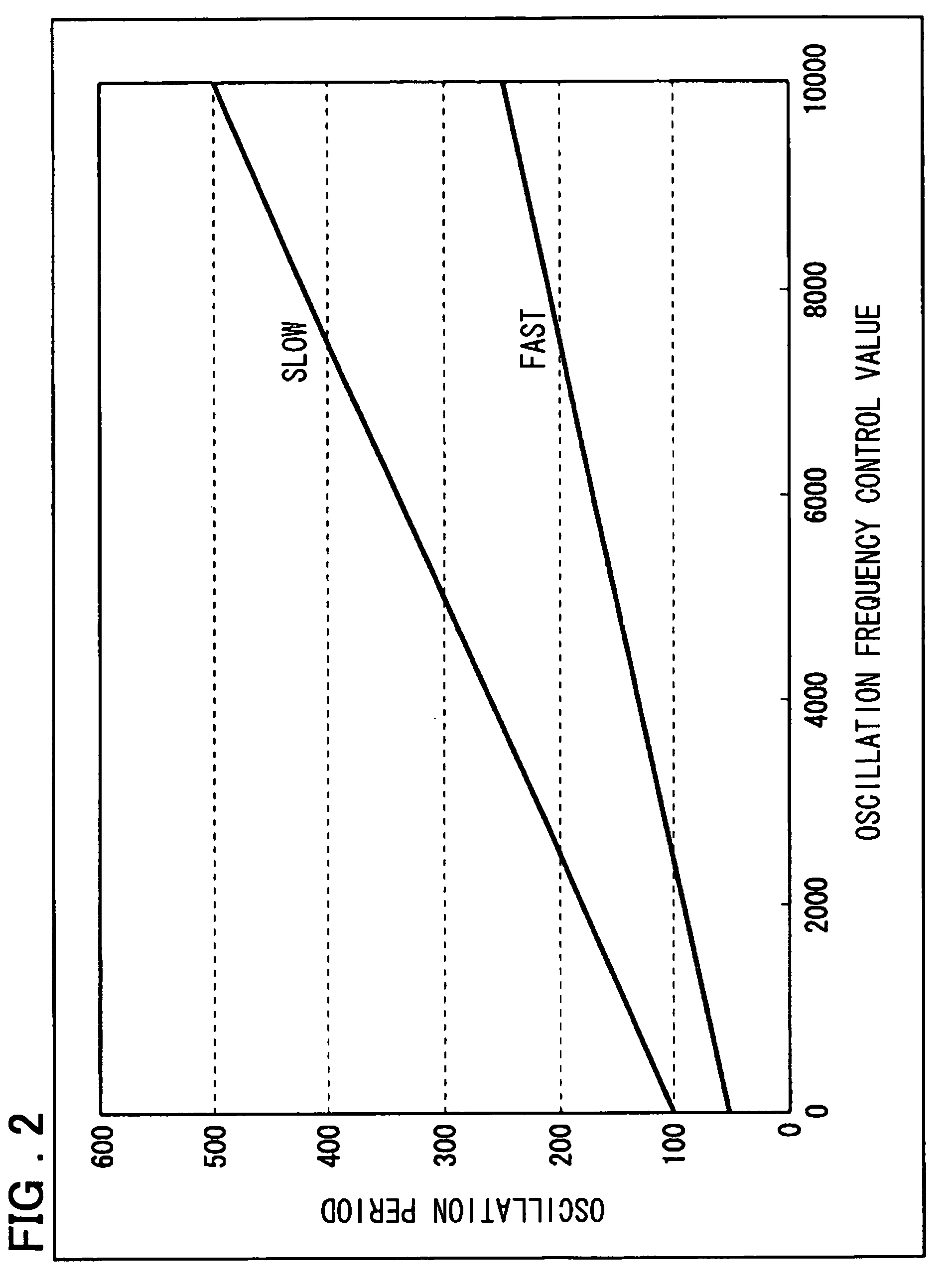
[0136]As shown in the first embodiment, the change rate of a delay caused by the manufacturing variations, supply voltage, and temperature used is constant. Thus, the B should be determined under a certain condition in advance.


PUM


Abstract

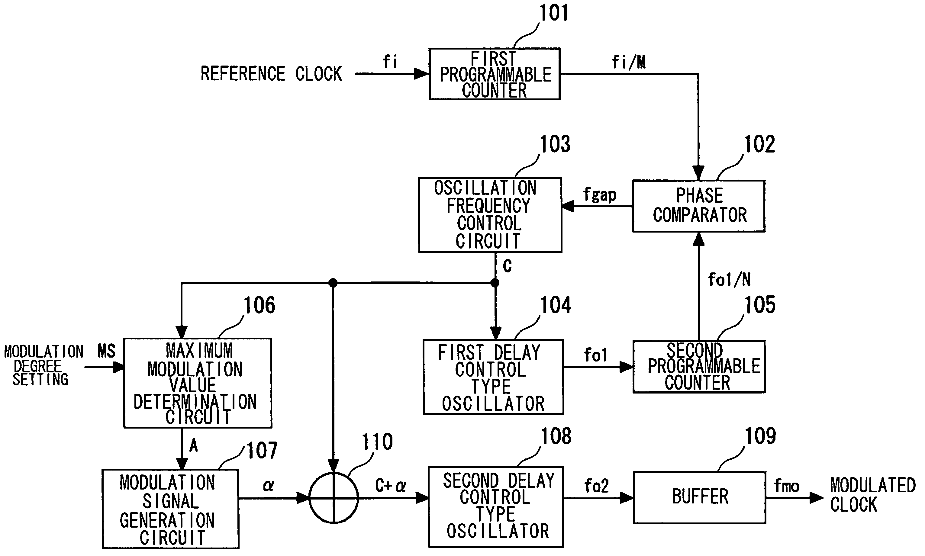
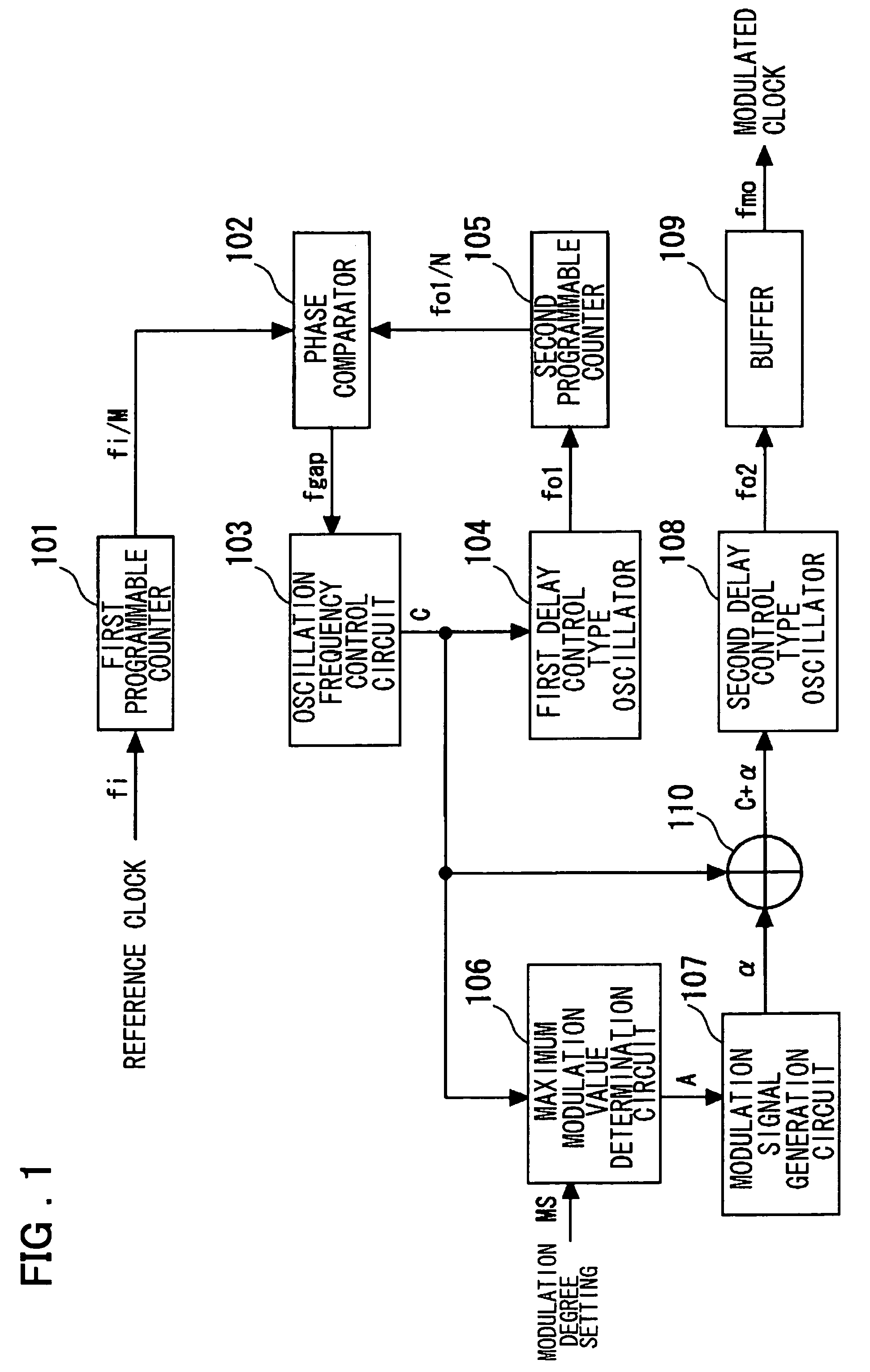
Disclosed is a spread spectrum clock generator which includes: a first delay control type oscillator that variably controls an oscillation period at a control period interval according to a control signal; a control circuit; a maximum modulation value determination circuit that determines a maximum modulation value from a predetermined value, a frequency control signal, and a given modulation degree setting signal; a modulation signal generation circuit that receives the maximum modulation value from the maximum modulation value determination circuit and generates a modulation control signal within the maximum modulation value; and a second delay control type oscillator that receives a value obtained by adding the modulation control signal from the modulation signal generation circuit to the frequency control signal as a control signal and variably controls the oscillation period of an output clock signal at the control period interval according to the control signal. The control circuit outputs the frequency control signal for variably controlling the oscillation period based on the result of phase comparison between a clock signal obtained by frequency dividing the output of the first delay control type oscillator and a frequency divided clock signal of a reference clock signal, performed by a phase comparator.

Description

FIELD OF THE INVENTION[0001]The present invention relates to a clock frequency spreading (Spread Spectrum Clock Generation: also referred to as “SSCG”) device, for reducing EMI (Electromagnetic Interference) of a semiconductor integrated circuit.BACKGROUND OF THE INVENTION[0002]With increased operation speed and improved functions of semiconductor integrated circuits, so-called EMI countermeasure for controlling radiated noise to be within a regulated value have especially become difficult. Thus, it sometimes happens that even if EMI countermeasure components, such as an EMI filter or a decoupling capacitor, are mounted on a printed circuit board, the regulated value cannot be cleared.[0003]Further, the mounting of the EMI countermeasure components on a printed circuit board may result in an increase in the occupied area thereof and the cost. In a situation where a lot of the semiconductor integrated circuits are synchronized with a clock signal, an SSCG technique for modulating a c...

Claims


Application Information

Patent Timeline
Patent Type & Authority Patents(United States)
IPC IPC(8): H04B1/00G06F1/04H03C3/00H03K5/156H03L7/081
CPCH03L7/0805H03L7/0997H03L7/0812H03L7/0816
Inventor YONEDA, SATOSHI
Owner RENESAS ELECTRONICS CORP
Learn More