

Optical recording medium, process for manufacturing the same, sputtering target for manufacturing the same, and optical recording process using the same
- Summary
- Abstract
- Description
- Claims
- Application Information
AI Technical Summary
Benefits of technology
Problems solved by technology
Method used
Image

Examples
examples
[0171]The present invention will be described in more detail with reference to the following EXAMPLES. It should be noted that the present invention is not limited to those EXAMPLES and conditions for manufacturing can be suitably changed or adjusted according to necessity.
Example A-1
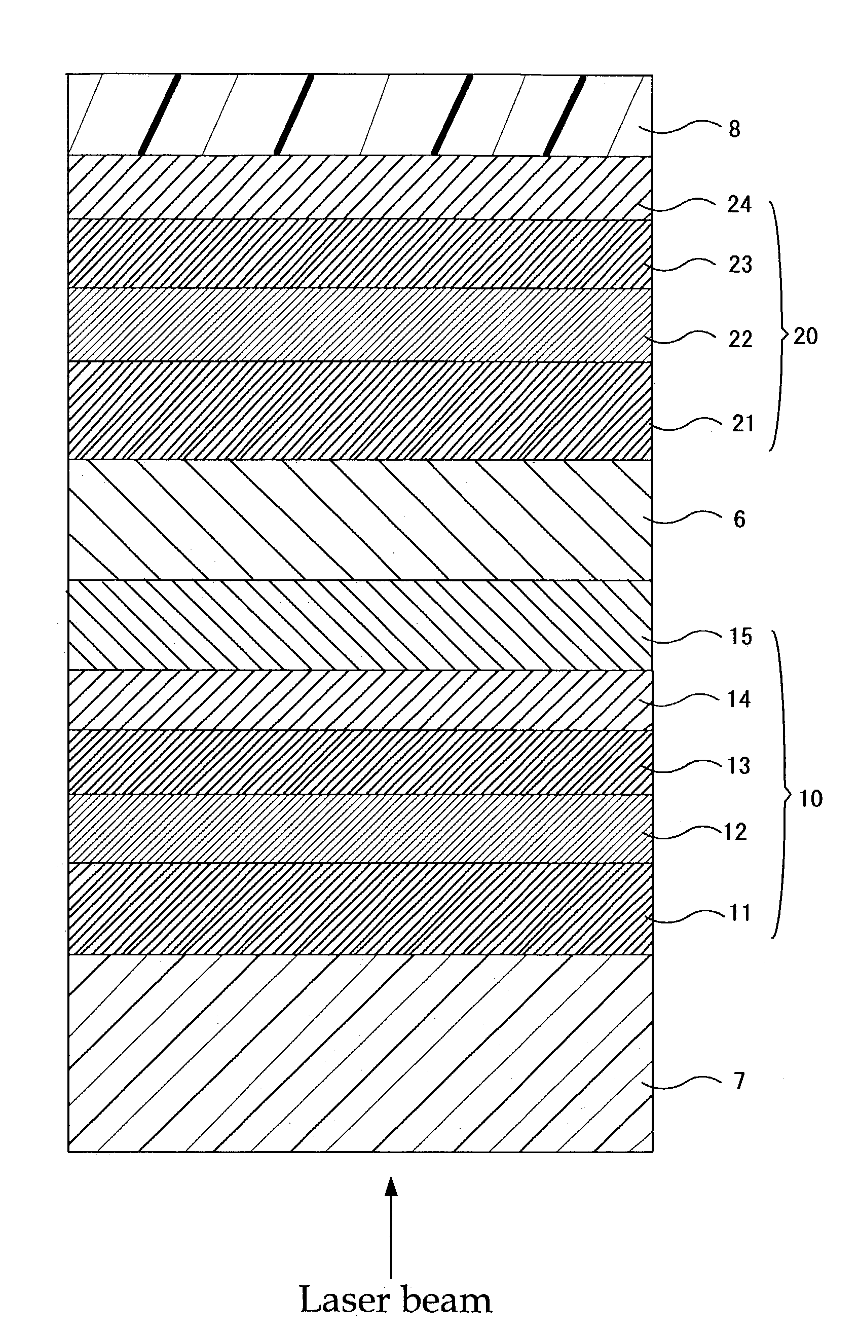
[0172]On a 0.6 mm thick polycarbonate substrate having a guiding groove which is formed of track pitch of 0.74 μm and of groove depth of 400 Å (40 nm), and also having a diameter of 120 mm, a 75 nm thick first protective layer comprising ZnS.SiO2 mixture target (in which SiO2 was 20 mol %), a 16 nm thick recording layer comprising Ga12Sb88 (atm %) alloy target, a 14 nm thick second protective layer comprising the same target as those for the first protective layer, and a 140 nm thick reflection layer comprising Ag—Pd (1 atm %)-Cu(1 atm %) target, were sequentially disposed in this order by the sputtering method.
[0173]As for the alloy target of the recording layer, a feed amount thereof was weighed befor...
example a-2
[0186]Optical recording media were manufactured in the same manner as in EXAMPLE A-1, except that the alloy target for recording was replaced with GaSb alloy having an identical composition to that of the recording layer shown in TABLE 2. Thereafter, those optical recording media were subjected to initial crystallization as in EXAMPLE A-1.
[0187]With respect to these optical recording media, C / N ratios [ratio between noise (N) level and signal intensity (C: carrier) was measured by spectrum analyzer] after 10 time DOW (direct overwriting) of 3T under the same recording conditions as those of EXAMPLE A-1, are shown in TABLE 2, and FIG. 7. In order to implement a rewritable optical disc system, the C / N ratio is required to be at least 45 dB. If it is 50 dB or more, further stable system can be obtained.
[0188]
TABLE 2GaSbC / N ratio(dB) after 10 times(atm %)(atm %)DOW of 3T397—595511288551585502080452575—
[0189]Furthermore, optical recording media were manufactured in the same manner as in ...
example a-3
[0194]Optical recording media were manufactured in the same manner as in EXAMPLE A-1, except that the alloy target for recording was replaced with an alloy which was obtained by adding 5 atm % of each of Ag, In, Sn, Ge, to Ga12Sb88. Thereafter, the optical recording media were subjected to initial crystallization as in EXAMPLE A-1.
[0195]As for thus obtained four of the optical recording media, recording test was conducted in a similar manner as that of EXAMPLE A-1. The alloy to which Ag or In was added, was capable of reducing recording power required to obtain the same degree of modulation as that in the case of recording using Ga12Sb88 alone, with Pw of 30 mW at the recording linear velocity of 28 m / s. When Ag was added, the recording power was reduced by 10%, and when In was added, it was reduced by 13% or less.
[0196]With a criteria for 45 dB or more for the C / N ratio, however, an alloy having the composition ratio of Ga12Sb88 alone enabled recording at a linear velocity of 36 m / ...
PUM
| Property | Measurement | Unit |
|---|---|---|
| Fraction | aaaaa | aaaaa |
| Thickness | aaaaa | aaaaa |
| Thickness | aaaaa | aaaaa |
Abstract
Description
Claims
Application Information