

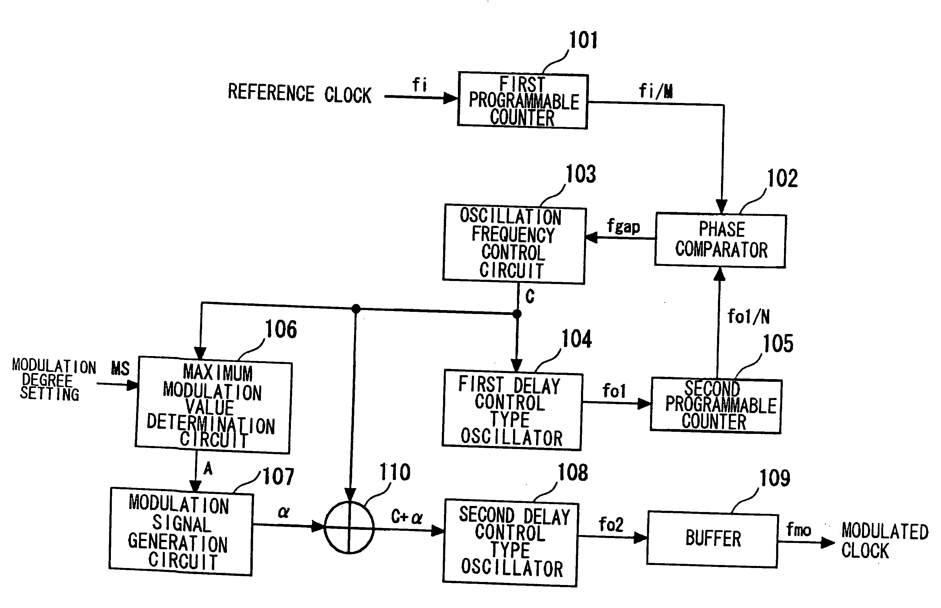
Spread Spectrum clock generator
a clock generator and spread spectrum technology, applied in the direction of generating/distributing signals, pulse techniques, multiplex communication, etc., can solve the problems of circuits that supply clocks, circuits that cannot achieve desired modulation, and increase the frequency of clocks, so as to prevent the reduction of emi reduction effect and reduce the component used for emi measures
- Summary
- Abstract
- Description
- Claims
- Application Information
AI Technical Summary
Benefits of technology
Problems solved by technology
Method used
Image

Examples
third embodiment
[0120]As the present invention, by repeating transition of the modulation control signal α only in a negative direction, such as 0, −1, . . . , −(A−1), −A, −(A−1), . . . −1, 0, −1 . . . , and the like, modulation of a up-spread type to a high frequency can be implemented.
[0121]Further, the transition of the modulation control signal a should be just in the range of the maximum value A. The pattern of the transition is not limited to those described above. Accommodation to various systems thereby becomes readily possible.
[0122]FIG. 7 is a diagram showing a configuration of a fourth embodiment of the present invention. Referring to FIG. 7, a third program counter III is provided in a stage subsequent to the second delay control type oscillator 108 in the first embodiment in FIG. 1. The third programmable counter III frequency divides the output of the second delay control type oscillator 108 by L. In the frequency division by L, the period which provides a basis for the frequency divi...
fourth embodiment
[0123]In the present invention, the frequency band of an output modulated clock can be expanded without expanding the frequency bands of the delay control type oscillators. Thus, an increase in the area is small because a low frequency band is handled.
[0124]Next, other embodiment of the present invention will be described. FIG. 8 is a diagram showing a configuration of a fifth embodiment of the present invention. The fifth embodiment of the present invention shows a case where the invention has been applied to a delay-type phase adjustment circuit (DLL: Delay Locked Loop).
[0125]In the delay-type phase adjustment circuit, a phase comparator 202 and a delay control circuit 203 perform an adjustment operation so that the delay value of a first variable delay circuit 201 becomes the length of one period of a received clock signal RCLK.
[0126]A second variable delay circuit 205 has the same characteristics as the first variable delay circuit 201. In order to output a desired phase set by ...
first embodiment
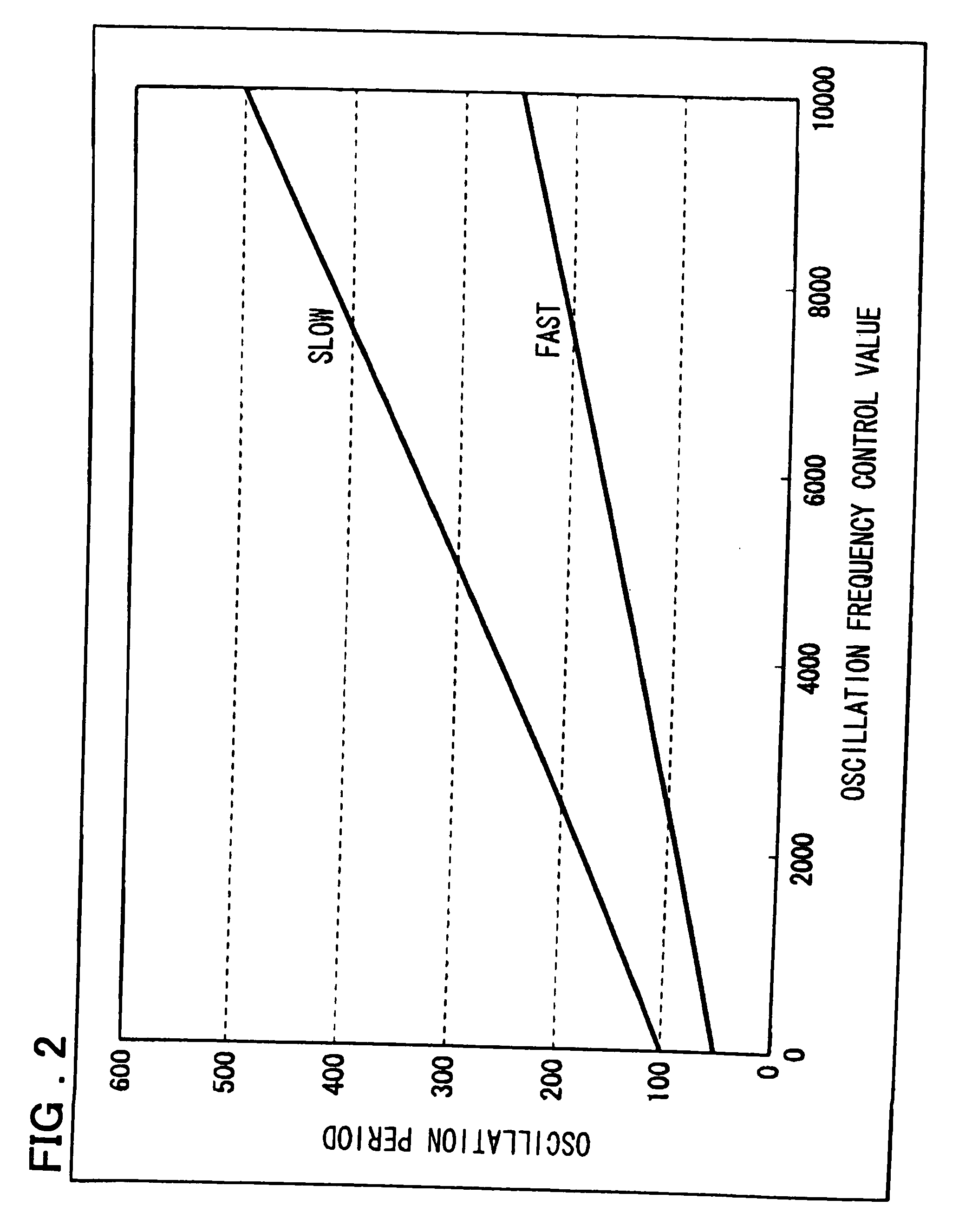
[0136]As shown in the first embodiment, the change rate of a delay caused by the manufacturing variations, supply voltage, and temperature used is constant. Thus, the B should be determined under a certain condition in advance.
PUM
 Abstract
Description
Claims
Application Information