Semiconductor device and method for manufacturing same

a semiconductor and semiconductor technology, applied in the field of semiconductor devices, can solve the problems of reducing affecting the service life of carriers, so as to achieve the effect of improving the mobility of carriers in the channel and high breakdown voltag

Active Publication Date: 2009-11-24
ROHM CO LTD
View PDF18 Cites 3 Cited by
  • Summary
  • Abstract
  • Description
  • Claims
  • Application Information

AI Technical Summary

Benefits of technology

[0006]It is therefore an object of the present invention to provide a semiconductor device having a structure which ensures both a higher breakdown voltage for suppression of punch-through and an improved carrier mobility in a channel at the same time, and to provide a manufacturing method of the semiconductor device.
[0008]With this arrangement, the deep portion of the impurity region has a higher second-conductivity impurity concentration, so that a depletion layer is prevented from spreading into the impurity region from a boundary between the impurity region and the underlying silicon carbide semiconductor epitaxial layer. On the other hand, the near surface of the impurity concentration, so that carriers moving in a channel region formed in a surface portion of the impurity region are less liable to be scattered. Thus, the mobility of the carriers in the channel can be kept high. This makes it possible to ensure both a high breakdown voltage for suppression of punch-through and an improved carrier mobility in the channel at the same time.
[0010]A second-conductivity impurity concentration in an outermost surface portion of the impurity region is preferably controlled to be lower than a first-conductivity impurity concentration in the silicon carbide semiconductor epitaxial layer. Thus, the second-conductivity impurity concentration in the outermost surface portion of the impurity region is lower than the first-conductivity impurity concentration in the silicon carbide semiconductor epitaxial layer, so that an accumulation MOSFET structure can be provided in which a first conductivity appears in the surface portion (channel region) of the impurity region and the channel region of the first conductivity serves as an accumulation layer. Therefore, a threshold voltage is reduced, and the carrier mobility in the channel is further improved.

Problems solved by technology

When the deep portion of the p-type impurity region has a lower impurity concentration, a depletion layer is liable to spread into the p-type impurity region from the boundary between the p-type impurity region and the n−-type SiC semiconductor epitaxial layer, so that punch-through is liable to occur.
However, where the p-type impurity region has a high impurity concentration, carriers moving in a channel region are liable to be scattered.
This disadvantageously reduces the carrier mobility in the channel (increases the ON resistance).

Method used


Image

  • Semiconductor device and method for manufacturing same
  • Semiconductor device and method for manufacturing same
  • Semiconductor device and method for manufacturing same

Examples


Embodiment Construction

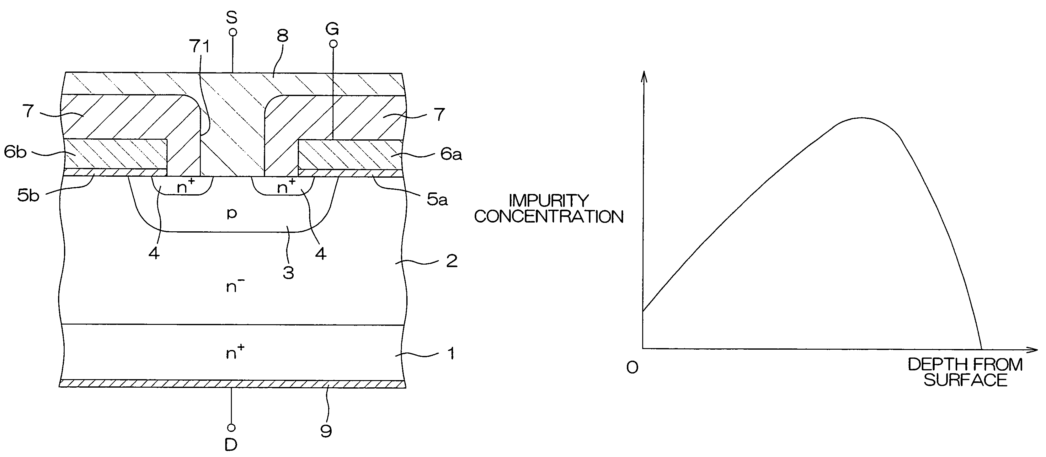
[0023]FIG. 1 is a sectional view schematically illustrating a construction of a semiconductor device according to an embodiment of the present invention. The semiconductor device is a double diffused MOSFET, and employs an n+-type SiC semiconductor substrate 1 as a semiconductor substrate.

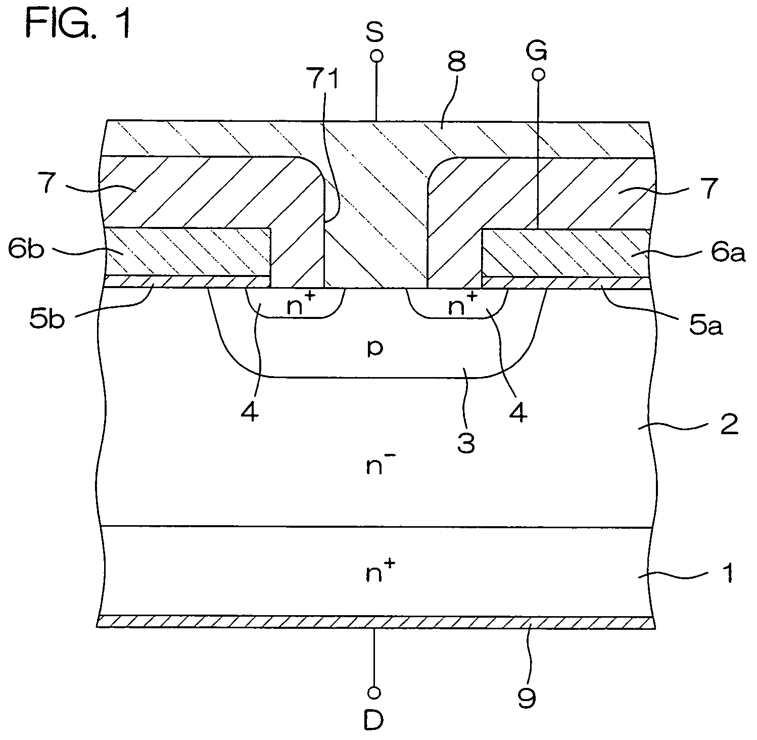
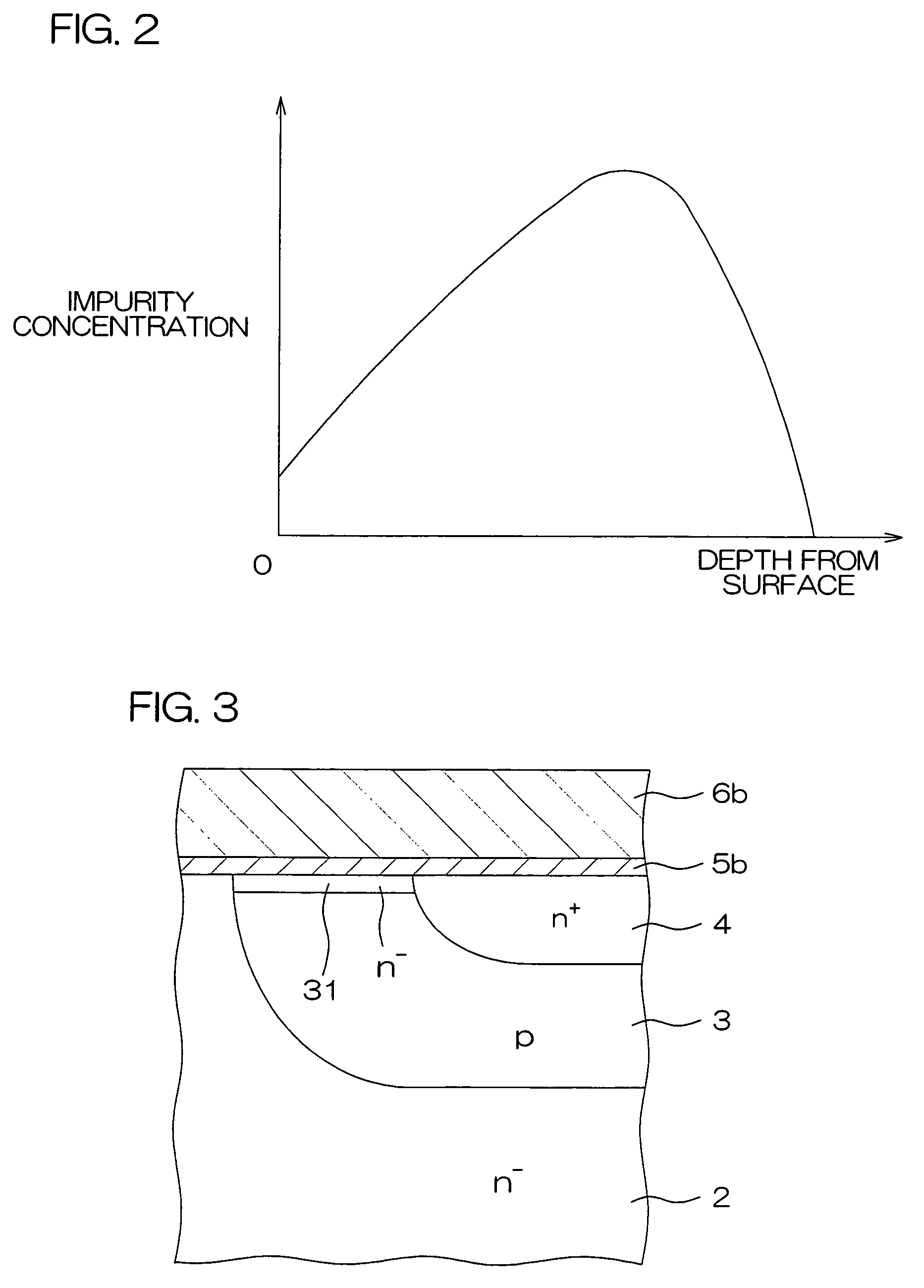
[0024]An n−-type SiC semiconductor epitaxial layer 2 having a lower impurity concentration than the n+-type SiC semiconductor substrate 1 is provided on a surface of the n+-type SiC semiconductor substrate 1. A p-type impurity region 3 having a rectangular shape as seen in plan, for example, is provided in a surface portion of the n−-type SiC semiconductor epitaxial layer 2. Further, an n+-type impurity region 4 having a rectangular frame shape as seen in plan is provided in the p-type impurity region 3 in properly spaced relation from peripheral edges of the p-type impurity region 3. The p-type impurity region 3 has a depth of 0.5 to 0.7 μm from a surface of the n−-type SiC semiconductor epitaxial...


PUM

PropertyMeasurementUnit
depthaaaaaaaaaa
depthaaaaaaaaaa
thicknessaaaaaaaaaa

Abstract

A semiconductor device of a double diffused MOS structure employing a silicon carbide semiconductor substrate. The semiconductor device comprises a silicon carbide semiconductor epitaxial layer provided on a surface of the silicon carbide semiconductor substrate and having a first conductivity which is the same conductivity as the silicon carbide semiconductor substrate, and an impurity region formed by doping a surface portion of the silicon carbide semiconductor epitaxial layer with an impurity of a second conductivity, the impurity region having a profile such that a near surface thereof has a relatively low second-conductivity impurity concentration and a deep portion thereof has a relatively high second-conductivity impurity concentration.

Description

TECHNICAL FIELD[0001]The present invention relates to a semiconductor device of a double diffused MOS structure employing a silicon carbide semiconductor substrate, and a manufacturing method for the semiconductor device.BACKGROUND ART[0002]In a double diffused MOS (DMOS) FET employing a silicon carbide (SiC) semiconductor substrate, an n−-type SiC semiconductor epitaxial layer is provided on a surface of an n+-type SiC semiconductor substrate. A p-type impurity region is provided in a surface portion of the n−-type SiC semiconductor epitaxial layer, and an n+-type impurity region having an annular shape as seen in plan is provided in the p-type impurity region.[0003]FIG. 7 is a diagram illustrating an impurity profile in the p-type impurity region in the prior-art double diffused MOSFET. In the prior-art double diffused MOSFET, the p-type impurity region has a so-called box profile. That is, the profile in the p-type impurity region in the prior-art double diffused MOSFET is contro...

Claims


Application Information

Patent Timeline
Patent Type & Authority Patents(United States)
IPC IPC(8): H01L31/0312H01L21/04H01L21/336H01L29/10H01L29/78
CPCH01L29/7828H01L29/7802H01L29/7838H01L29/66068H01L29/1079H01L29/1095H01L29/1608
Inventor MIURA, MINEO
Owner ROHM CO LTD
Why Eureka
Try Eureka