
Electrically alterable non-volatile memory cells and arrays

a non-volatile, memory cell technology, applied in the field of non-volatile memory, can solve the problems of high voltage, charge leakage and retention failure, complex process technology for manufacturing memories, etc., and achieve the effect of improving electrically alterable memory cells and operation methods

Inactive Publication Date: 2009-12-01
WANG CHIH HSIN
View PDF30 Cites 22 Cited by
  • Summary
  • Abstract
  • Description
  • Claims
  • Application Information

AI Technical Summary

Benefits of technology

This approach reduces stress on insulators, enhances erase operation reliability, and allows for efficient, low-voltage erase operations without the need for high-voltage infrastructure, while maintaining high injection efficiency and preventing over-erase issues.

Problems solved by technology

Therefore, it complicates process technology for manufacturing the memories.
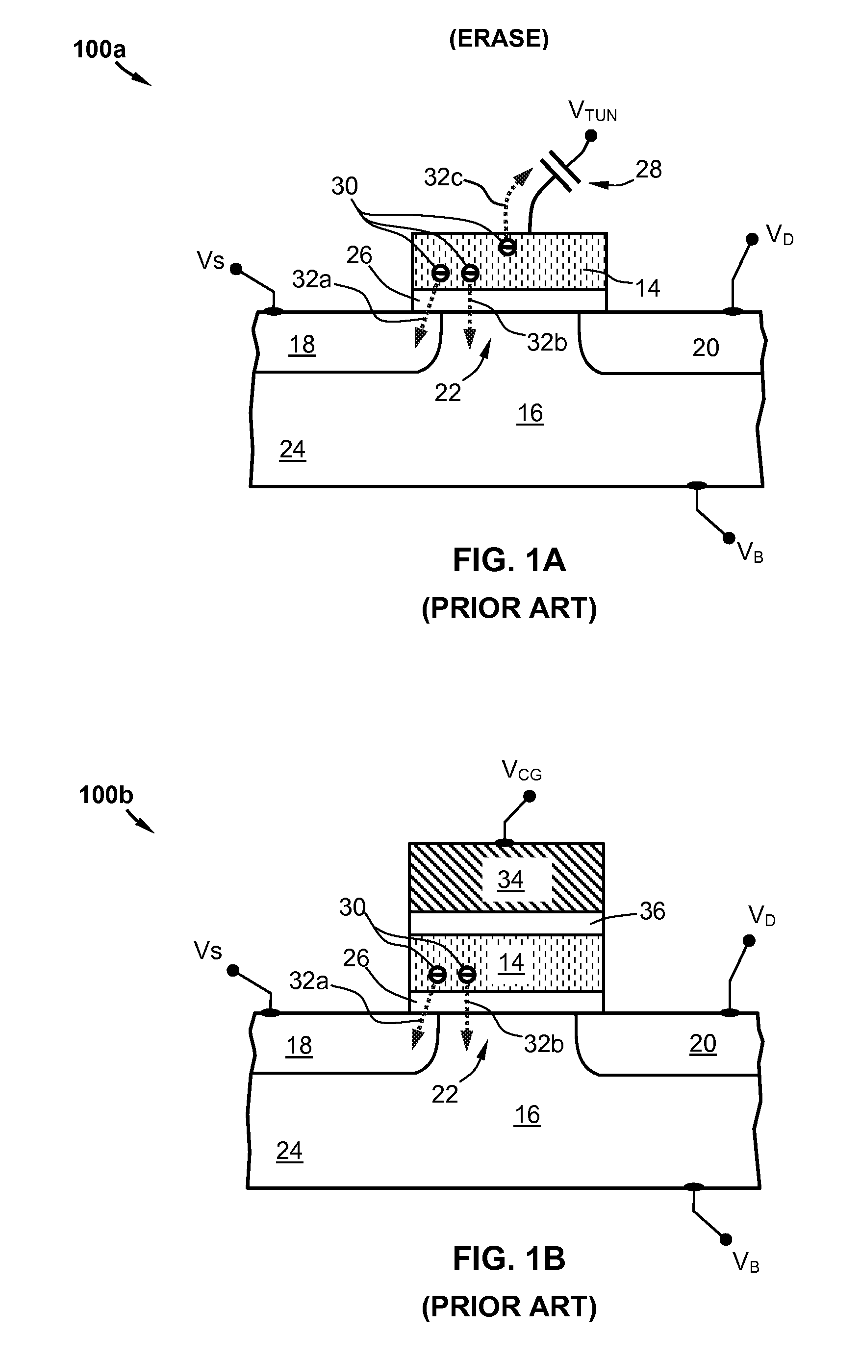
Further, the FN mechanism unavoidably introduces stress field in the range of about 10 MV / cm to the surrounding insulator, and results in charge leakage and retention failure even when memory cells are under a low field condition.
It is believed that the high voltage demands stringent control on the quality of the surrounding insulators.
The memories operated under the mechanism thus are vulnerable to manufacturing and reliability problems.
Such erase method is believe suffered from the problems of low injection efficiency (Here, the term “injection efficiency” is defined as the ratio of the number of charge carriers entering into FG to the number of charge carriers supplied by the source).
One of the major problems for UV treatment is that the erase operation requires erasure of the entire memory device by application of UV light even erase is made for changing the content of only a single byte.
The process is tedious and adds inconvenience in product applications.

Method used


Image

  • Electrically alterable non-volatile memory cells and arrays
  • Electrically alterable non-volatile memory cells and arrays
  • Electrically alterable non-volatile memory cells and arrays

Examples


Embodiment Construction

[0043]Embodiments of the present invention described in the following detailed description are directed at memory cell structures and operation methods. Those of ordinary skill in the art will realize that the detailed description is illustrative only and is not intended to restrict the scope of the claimed inventions in any way. Other embodiments of the present invention, beyond those embodiments described in the detailed descriptions, will readily suggest themselves to those of ordinary skill in the art having the benefit of this disclosure. Reference will now be made in detail to implementations of the present invention as illustrated in the accompanying drawings. Where appropriate, the same reference indicators will be used throughout the drawings and the following detailed description to refer to the same or similar parts.

[0044]As used herein, the symbol p+ indicates a heavily doped semiconductor material of p-type conductivity typically having a doping level of p-type impuriti...


PUM


Abstract

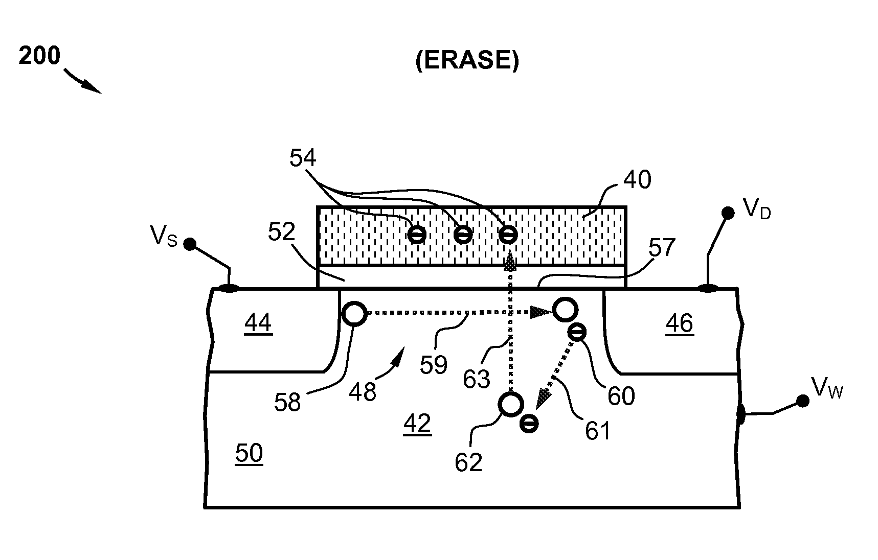
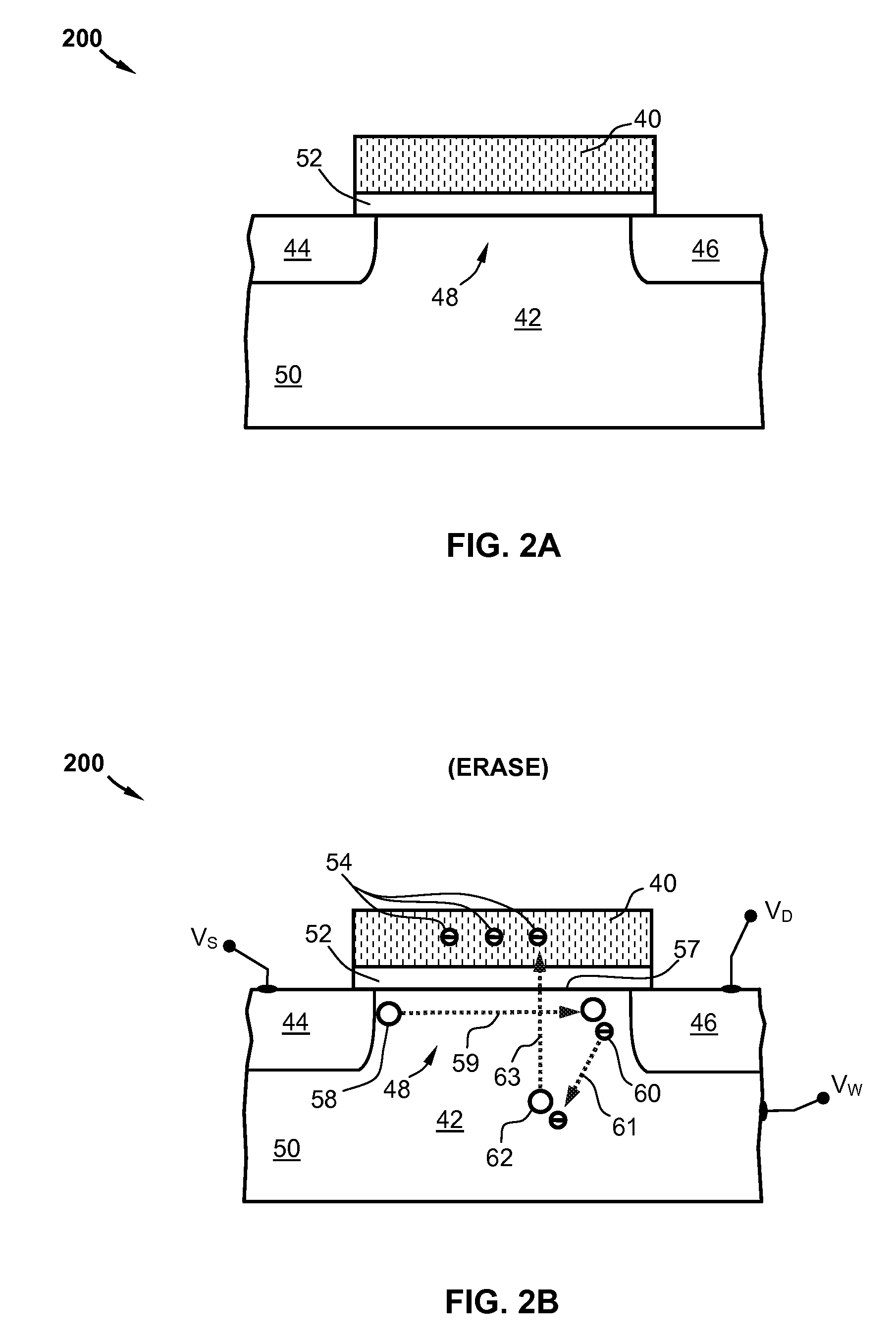
Nonvolatile memory cells and array are provided. The memory cell comprises a body, a source, a drain, and a charge storage region. The body comprises an n-type conductivity and is formed in a well of the n-type conductivity. The source and the drain have p-type conductivity and are formed in the well with a channel of the body defined therebetween. The charge storage region is disposed over and insulated from the channel by a channel insulator. Each cell further comprises a bias setting having a source voltage applied to the source, a well voltage applied to the well, and a drain voltage applied to the drain. A bias configuration for an erase operation of the memory cell is further provided, wherein the source voltage is sufficiently more negative with respect to the well voltage and is sufficiently more positive with respect to the drain voltage to inject hot holes onto the charge storage region. The cells can be arranged in row and column to form memory arrays and memory device.

Description

RELATED APPLICATIONS[0001]Cross-reference is made to U.S. patent application Ser. No. 10 / 962,288 filed on Oct. 8, 2004 and to U.S. patent application Ser. No. 10 / 919,555 filed on Aug. 16, 2004.TECHNICAL FIELD[0002]The present invention deals with non-volatile memory, and relates more specifically to Electrically Programmable Read Only Memories (EPROM) and Electrically Erasable and Programmable Read Only Memories (EEPROM). More particularly, the present invention relates to memory cell structure and method altering charge state of memory cells by employing mechanism injecting holes onto floating gate or charge storage sites of non-volatile memory cells for erase operation.BACKGROUND OF THE INVENTION[0003]Non-volatile semiconductor memory cells using a charge storage region to store charges and memory arrays of such non-volatile memory cells in a semiconductor substrate are well known in the art. The charge storage region or charge storage sites are electrically insulated from and cap...

Claims


Application Information

Patent Timeline
Patent Type & Authority Patents(United States)
IPC IPC(8): G11C11/34H01L29/788
CPCH01L27/115H01L29/7885H01L27/11558H01L29/42324H01L27/11521G11C16/0416G11C16/0433H10B41/60H10B69/00H10B41/30
Inventor WANG, CHIH-HSIN
Owner WANG CHIH HSIN
Learn More