Manufacturing method for semiconductor devices, and formation apparatus for semiconductor wafer dicing masks

a manufacturing method and semiconductor technology, applied in the direction of individual semiconductor device testing, semiconductor/solid-state device testing/measurement, instruments, etc., can solve the problems of affecting the uniform thickness of manufactured semiconductor devices, affecting the uniformity of dicing position portions, and affecting the quality of semiconductor devices, so as to achieve high-quality semiconductor devices and maintain the effect of uniform dicing position portions

Active Publication Date: 2009-12-08
PANASONIC CORP
View PDF10 Cites 158 Cited by
  • Summary
  • Abstract
  • Description
  • Claims
  • Application Information

AI Technical Summary

Benefits of technology

[0006]An object of the present invention is to provide, for solving the problem, a dicing method for semiconductor wafer capable of distinguishing flawed semiconductor devices from other semiconductor devices while preventing degradation of the quality of the respective semiconductor devices in a semiconductor wafer, a manufacturing method for semiconductor devices, and a formation apparatus for semiconductor wafer dicing masks for use during dicing of the semiconductor devices.
[0061]Moreover, by incorporating such semiconductor wafer dicing methods of the respective aspects in the manufacturing process of semiconductor devices, it becomes possible to provide a manufacturing method for semiconductor devices capable of covering acquisition of the position information for flawed semiconductor devices from the inspection process to dicing of the semiconductor wafer into the respective separate semiconductor devices performed together with formation of the bad marks.

Problems solved by technology

This causes such problem as degraded quality of semiconductor devices as the formation of the bad marks aiming at quality management of the semiconductor devices contrarily hinders the uniformity of the thickness of manufactured semiconductor devices.
Particularly, the thinned semiconductor wafer is often required a higher-level uniformity of the thickness, making occurrence of such a problem more prominent.

Method used


Image

  • Manufacturing method for semiconductor devices, and formation apparatus for semiconductor wafer dicing masks
  • Manufacturing method for semiconductor devices, and formation apparatus for semiconductor wafer dicing masks
  • Manufacturing method for semiconductor devices, and formation apparatus for semiconductor wafer dicing masks

Examples


Embodiment Construction

[0086]Before the description of the present invention proceeds, it is to be noted that like parts are designated by like reference numerals throughout the accompanying drawings.

[0087]Hereinbelow, the embodiment of the present invention will be described in detail with reference to the drawings.

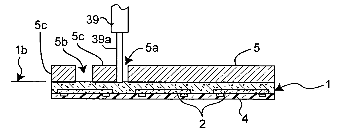
[0088]For describing a semiconductor wafer dicing method and a semiconductor device manufacturing method according to a first embodiment of the present invention, first, the structure of the apparatuses for use in the dicing method and the manufacturing method will be described.

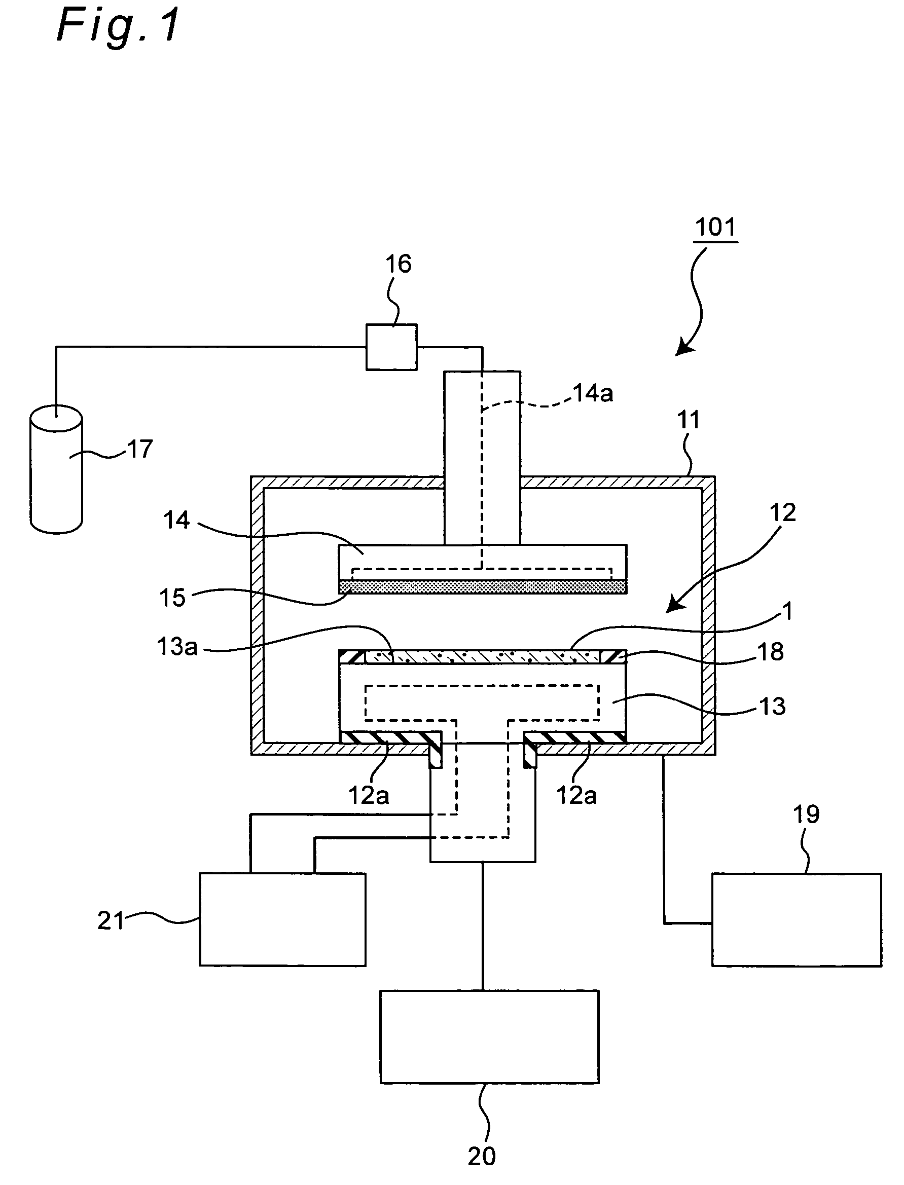
[0089]FIG. 1 shows a schematic diagram schematically showing the structure of a plasma processing apparatus 101 exemplifying the semiconductor wafer dicing apparatus for implementing the semiconductor wafer dicing method in the first embodiment. The plasma processing apparatus 101 applies plasma etching to a semiconductor wafer having a plurality of semiconductor devices formed thereon to conduct dicing (plasma dicing) ...


PUM


Abstract

On a mask placement-side surface of a semiconductor wafer in which a plurality of semiconductor devices are formed, a mask is placed, while dicing lines for dicing the semiconductor wafer into the respective separate semiconductor devices are defined and a surface of a flawed semiconductor device among the respective semiconductor devices is partially exposed, and then plasma etching is applied to the mask placement-side surface of the semiconductor wafer so as to dice the semiconductor wafer into the respective semiconductor devices along the defined dicing lines, and an exposed portion of the flawed semiconductor device is removed so as to form a removed portion as a flawed semiconductor device distinguishing mark.

Description

BACKGROUND OF THE INVENTION[0001]The present invention relates to a dicing method for a semiconductor wafer in which a semiconductor wafer with a plurality semiconductor devices formed thereon is diced into the respective separate semiconductor devices by application of plasma etching, a manufacturing method for semiconductor devices including such a dicing method involving the plasma etching as a part of its process, and a formation apparatus for semiconductor wafer dicing masks for forming semiconductor wafer dicing masks for defining dicing lines used for dicing of the respective separate semiconductor devices through the plasma etching.[0002]Conventionally, in manufacturing of such semiconductor devices, after a plurality of semiconductor devices are formed on a circuit formation face of a semiconductor wafer, the formed semiconductor devices undergo an inspection (mainly an inspection of electric characteristic), and based on the result of quality check, flawed (bad) semiconduc...

Claims


Application Information

Patent Timeline
Patent Type & Authority Patents(United States)
IPC IPC(8): H01L21/00
CPCH01L21/6835H01L21/6836H01L21/78H01L23/544H01L2221/68327H01L2221/6834H01L2924/0002H01L2221/68359H01L2223/54473H01L2924/00
Inventor HAJI, HIROSHIARITA, KIYOSHINISHINAKA, TERUAKI
Owner PANASONIC CORP
Why Eureka
Try Eureka