Manufacturing method of organic thin-film transistors and equipment for manufacturing the same

a manufacturing method and technology of organic thin-film transistors, applied in the direction of thermoelectric devices, electrolytic capacitors, coatings, etc., can solve the problems of complex equipment, high cost, and inability to expect sufficient crystal growth, and achieve the effect of complex equipment and high cos

Inactive Publication Date: 2009-12-22
HITACHI LTD
View PDF16 Cites 0 Cited by
  • Summary
  • Abstract
  • Description
  • Claims
  • Application Information

AI Technical Summary

Benefits of technology

[0005]In the forming of a semiconductor layer using an organic semiconductor material disclosed in Patent Document 1, pentacene is subjected to vacuum deposition to form a semiconductor layer. To do this, equipment for evacuation has to be required, such as a vacuum vessel, a pump, and others, resulting in a complex equipment and high cost.
[0007]The present invention is devised in view of the above inconveniences of the conventional technology. An object of the present invention is to increase productivity of organic thin-film transistors. Another object of the present invention is to achieve a high-performance organic thin-film transistor.
[0012]According to the present invention, the substrate is coated with a semiconductor and heated on the same carrying route, thereby increasing productivity of organic thin-film transistors. Also, the semiconductor layer is heated to control a drying speed (rate) of the semiconductor layer, thereby achieving high-performance organic thin-film transistors. Furthermore, the back surface side of the substrate is used for carrying and heating, thereby preventing organic contamination of the semiconductor layer and wiring from a carrier device and a heating device.

Problems solved by technology

To do this, equipment for evacuation has to be required, such as a vacuum vessel, a pump, and others, resulting in a complex equipment and high cost.
In the method of forming a transistor material disclosed in Patent Document 2, when liquid pentacene is coated at room temperature, a sufficient crystal growth cannot be expected.
However, since it is difficult to simultaneously perform coating and heating, productivity in the semiconductor layer forming process is low.
Also, it is difficult to accurately control crystal growth.
Therefore, making properties of the coating film uniform and simplifying the equipment are not sufficiently taken into consideration.

Method used


Image

  • Manufacturing method of organic thin-film transistors and equipment for manufacturing the same
  • Manufacturing method of organic thin-film transistors and equipment for manufacturing the same
  • Manufacturing method of organic thin-film transistors and equipment for manufacturing the same

Examples


Embodiment Construction

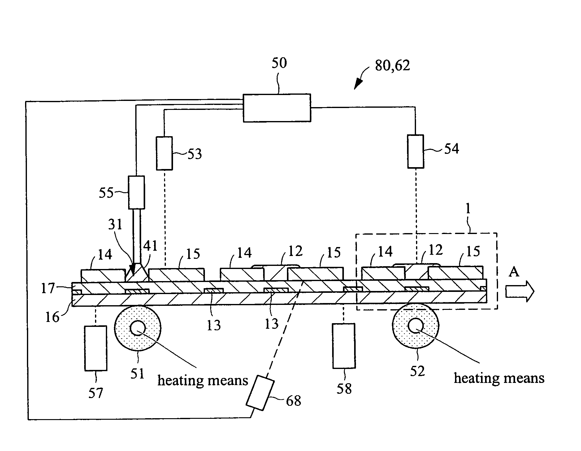
[0023]The organic thin-film transistor manufacturing method according to the present invention is described below with reference to the drawings. FIG. 1 as a vertical cross sectional view of one embodiment of an equipment 80 that manufactures an-organic thin-film transistor (TFT) 1. On carrier rollers 51 and 52 disposed so as to be spaced apart from each other, a substrate 16 to be processed is placed. The carrier rollers 51 and 52 carry the substrate 16 intermittently in a direction denoted by an arrow A. On the upper surface of the substrate 16, an organic thin-film transistor 1 is formed, details of which are shown in FIGS. 6A and 6B. FIG. 6A is a cross-sectional view of the organic thin-film transistor 1, whilst FIG. 6B is a plan view thereof. Here, a surface on which a semiconductor layer 12 is formed is referred to as a front surface of the substrate 16, whilst a surface opposite thereto is referred to as a back surface of the substrate 16. A gate electrode 13 is formed at a p...


PUM

PropertyMeasurementUnit
contact angleaaaaaaaaaa
thicknessaaaaaaaaaa

Abstract

To increase productivity of organic thin-film transistors, in an organic thin-film transistor manufacturing equipment, a liquid containing at least either one of a wiring material and a semiconductor material is coated on a substrate to form a number of organic thin-film transistors. Substrate carrying means carry the substrate. The substrate is heated by a first heating means, and the temperature of the substrate is controlled by a controller. The liquid containing at least either one of the wiring material and the semiconductor material is heated by a second heating means, and the temperature of this liquid is controlled also by the controller.

Description

CROSS-REFERENCE TO RELATED APPLICATION[0001]The present application claims priority from Japanese Patent Application No. JP 2006-025197 filed on Feb. 2, 2006, the content of which is hereby incorporated by reference into this application.TECHNICAL FIELD OF THE INVENTION[0002]The present invention relates to a manufacturing method of organic thin-film transistors and an equipment for manufacturing the same.BACKGROUND OF THE INVENTION[0003]An example of a conventional organic thin-film transistor is disclosed in Japanese Patent Application Laid-Open Publication No. 2001-94107 (Patent Document 1) In the organic thin-film transistor disclosed in this gazette, in order to obtain high mobility, a gate electrode, a gate insulator, an organic semiconductor layer, a source electrode, a drain electrode, and a protection film are formed on the surface of a substrate, and a contact angle of pure water on the surface of the gate insulating layer is set equal to or larger than 50 degrees and equa...

Claims


Application Information

Patent Timeline
Patent Type & Authority Patents(United States)
IPC IPC(8): H01L35/24
CPCH01L21/67109H01L21/6715H01L21/67248H01L51/0003H01L51/0545H01L51/0027H01L51/0541H10K71/12H10K71/421H10K10/466H10K10/464
Inventor INOUE, TOMOHIRODOI, AKIRAANDO, MASAHIKO
Owner HITACHI LTD
Why Eureka
Try Eureka