Reference voltage generating circuit and semiconductor integrated circuit device

a voltage generation circuit and reference voltage technology, applied in the direction of digital storage, process and machine control, instruments, etc., can solve the problems of complex operation, increase in error of access time for semiconductor memory, and delay time actually varies for each semiconductor memory, so as to suppress the effect of delay time fluctuation, suppressing the increase in consumption curren

Active Publication Date: 2010-01-05
MICRON TECH INC
View PDF15 Cites 10 Cited by
  • Summary
  • Abstract
  • Description
  • Claims
  • Application Information

AI Technical Summary

Benefits of technology

[0007]An object of the present invention is to provide a reference voltage generating circuit and a semiconductor integrated circuit device capable of reducing fluctuation of delay time while suppressing consumption current, in which a reference voltage corrected to reduce an influence of the variation of characteristics due to process fluctuation and temperature fluctuation is generated in a circuit using low Vt transistors.
[0009]According to the reference voltage generating circuit of the present invention, a pair of low threshold voltage MOS transistors included in the monitor circuit has different characteristics of the threshold voltage and the current, which is cause by the process fluctuation, and thus the monitor current and a voltage drop of the monitor circuit change according to the characteristics. Then, the reference voltage generated at one end of the monitor circuit is corrected within a predetermined range from the predetermined center value according to the change of the voltage drop using the constant voltage as a reference at the other end of the monitor circuit. At this point, by appropriately adjusting design conditions of the pair of low threshold voltage MOS transistors and the resistor, consumption current and delay characteristics of the low threshold voltage MOS transistors can be appropriately controlled by the correction of the reference voltage. Then, when a circuit including the low threshold voltage MOS transistors is operated using the reference voltage, fluctuation of the delay time due to the process fluctuation can be reduced while suppressing the consumption current.
[0013]According to the semiconductor integrated circuit device of the present invention, the temperature sensor circuit and the plurality of reference voltage generating circuits are provided, each of the reference voltage generating circuits is adjusted corresponding to the temperature detected by the temperature sensor circuit, and each of the reference voltage generating circuits is selectively operated corresponding to a detected result. Thus, it is possible to suppress an increase in consumption current and fluctuation of the delay time due to an influence of temperature fluctuation in addition to the process fluctuation in the semiconductor integrated circuit device.
[0019]As described above, according to the reference voltage generating circuit of the present invention, a monitor circuit including a pair of low threshold voltage MOS transistors is appropriately adjusted, a voltage value of a reference voltage generated at one end according to a change of a monitor current can be automatically corrected, and fluctuation of a delay time due to process fluctuation and an increase in consumption current can be suppressed. Further, according to the semiconductor integrated circuit device of the present invention, a plurality of the reference voltage generating circuits is provided corresponding to temperatures, and each reference voltage generating circuit is selectively operated corresponding to a detected result of the temperature sensor circuit. Therefore, in a circuit to which an internal power supply voltage based on the reference voltage is supplied, it is possible to suppress an increase in consumption current and fluctuation of the delay time due to temperature fluctuation in addition to process fluctuation. Particularly, when the present invention is applied to an access path in the semiconductor integrated circuit device including a memory circuit, malfunction due to an error of an access time can be prevented by reducing the fluctuation of the delay time.

Problems solved by technology

Generally, complex operation needs to be performed when accessing the semiconductor memory, and delay time for the operation should be considered.
However, the delay time actually varies for each semiconductor memory due to process fluctuation.
Then, delay difference when comparing a condition to maximize the delay time and a condition to minimize the delay time is increased, and this causes a problem of an increase in error of an access time for the semiconductor memory.
However, variations of the low Vt transistor characteristics due to the process fluctuation causes various problems in the above conventional method.
When the threshold voltage of the low Vt transistor varies downward, the operation delay is reduced, but both operation current and leak current are increased, thereby increasing consumption current.
Meanwhile, when the threshold voltage of the low Vt transistor varies upward, the consumption current is reduced, but the operation delay is increased.
In this case, if a power supply voltage of the low Vt transistors is lowered for the purpose of a reduction in the consumption current, the influence of the variation of the above threshold voltage is relatively increased, thereby further increasing the fluctuation of the delay time of the circuit.
In this manner, it is a problem that in the conventional semiconductor integrated circuit device, it is difficult to reduce the fluctuation of the delay time in the circuit due to the process fluctuation and the temperature fluctuation without an increase in the consumption current, and the error of the access time or the like occurs.

Method used


Image

  • Reference voltage generating circuit and semiconductor integrated circuit device
  • Reference voltage generating circuit and semiconductor integrated circuit device
  • Reference voltage generating circuit and semiconductor integrated circuit device

Examples


Embodiment Construction

[0034]A preferred embodiment of the present invention will be described with reference to the accompanying drawings. In the embodiment, a case of applying the present invention to a DRAM as a semiconductor integrated circuit device will be described.

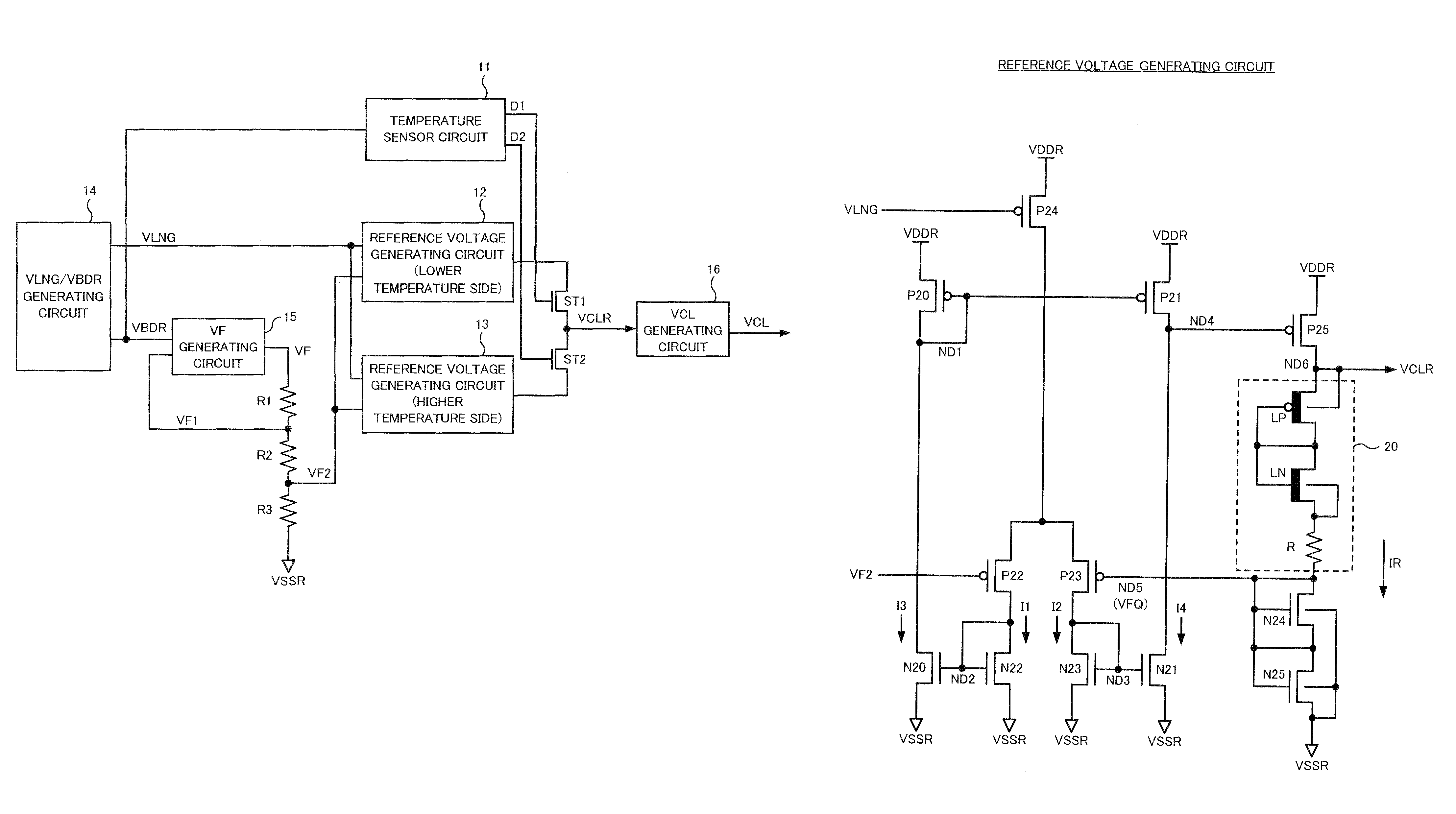
[0035]FIG. 1 is a block diagram showing a configuration of a principal part for correcting a reference voltage VCLR in the DRAM of the embodiment. The reference voltage VCLR is used as a reference for an internal power supply voltage VCL supplied to principal circuits of the DRAM of the embodiment. The principal part as shown in FIG. 1 includes a temperature sensor circuit 11, two reference voltage generating circuits 12 and 13, a VLNG / VBDR generating circuit 14, a VF generating circuit 15, a VCL generating circuit 16, two switch transistors ST1 and ST2, and three resistors R1, R2 and R3.

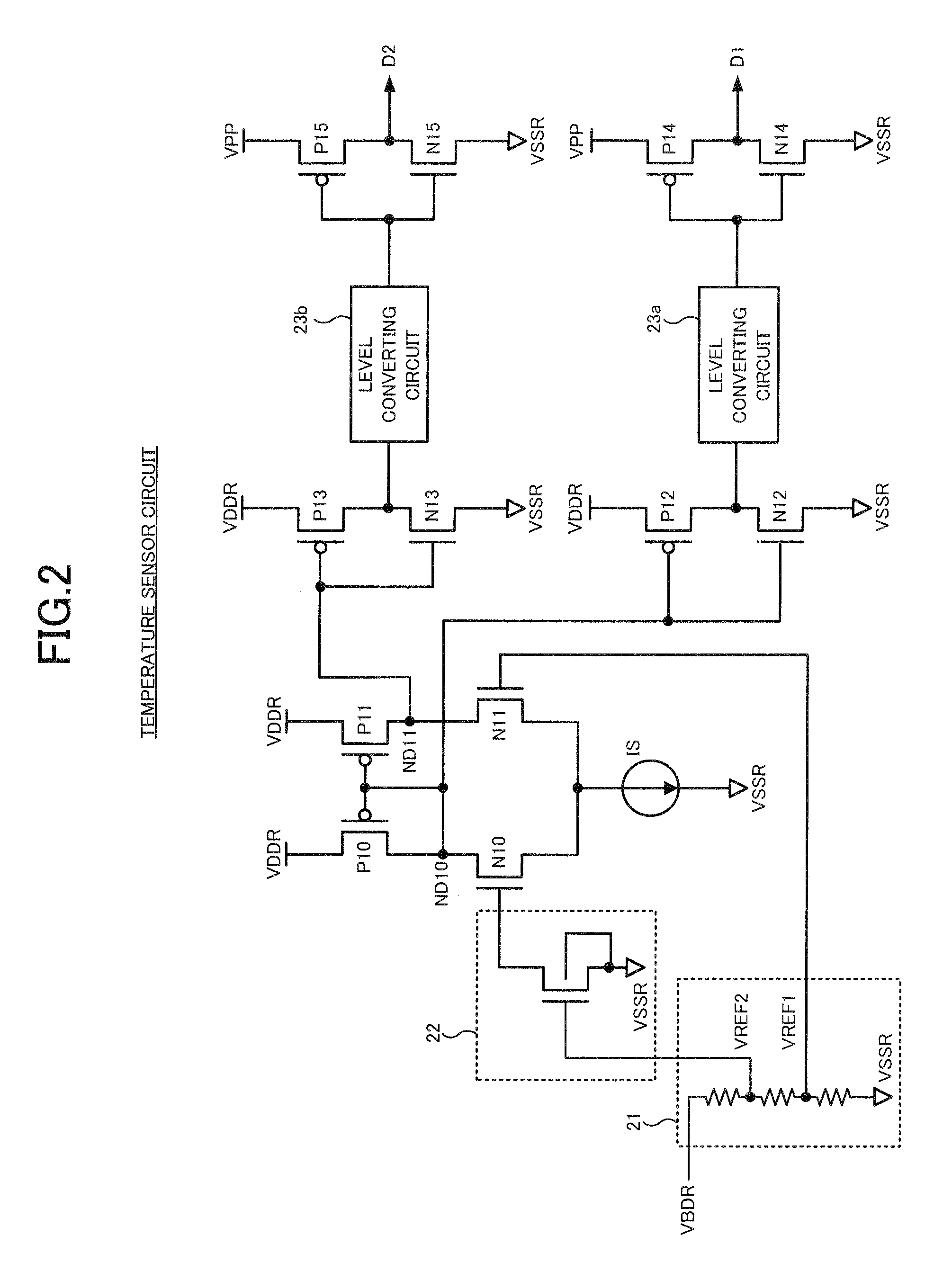
[0036]In the above configuration, the temperature sensor circuit 11 detects a temperature as a binary value indicating a high temperature or a low tempe...


PUM


Abstract

A reference voltage generating circuit comprises: a monitor circuit, including a low threshold voltage PMOS transistor, a low threshold voltage NMOS transistor, and a resistor having a predetermined resistance which are connected in series, for generating a reference voltage at one end; and an additional circuit for supplying a monitor current to the monitor circuit and for controlling the other end of the monitor circuit to be at a constant voltage, wherein a voltage value of the reference voltage is corrected within a range corresponding to a process fluctuation from a predetermined center value, based on the monitor current changing in response to the process fluctuation.

Description

BACKGROUND OF THE INVENTION[0001]1. Field of the Invention[0002]The present invention relates to a technical field of a semiconductor integrated circuit device configured using a large number of MOS transistors, and particularly relates to a technical field of a semiconductor memory device such as a DRAM (Dynamic Random Access Memory) which is accessed through a signal path using a large number of MOS transistors.[0003]2. Description of the Related Art[0004]In recent years, as performance of a semiconductor integrated circuit device is improved, high speed operation and low voltage operation are required. Particularly, a semiconductor memory such as a DRAM has enabled high frequency operation, high speed access and low voltage operation due to finer manufacturing process, and higher performance is strongly required (e.g., see Japanese Patent Application Laid-open No. 2000-11649). Generally, complex operation needs to be performed when accessing the semiconductor memory, and delay ti...

Claims


Application Information

Patent Timeline
Patent Type & Authority Patents(United States)
IPC IPC(8): G05F1/10
CPCG11C5/147G11C7/04G11C11/4074G11C11/4099
Inventor RIHO, YOSHIRO
Owner MICRON TECH INC
Why Eureka
Try Eureka