Pixel circuit and display apparatus

a pixel circuit and display apparatus technology, applied in static indicating devices, instruments, electroluminescent light sources, etc., can solve problems such as difficulty in producing large-scale, high-definition display apparatuses, and achieve stable corrective action of pixel circuits, easy control of pixel array operation, and increase of the fixed margin for a mobility correcting period

Active Publication Date: 2010-02-09
SONY CORP
View PDF16 Cites 55 Cited by
  • Summary
  • Abstract
  • Description
  • Claims
  • Application Information

AI Technical Summary

Benefits of technology

[0012]It is desirable to provide a pixel circuit and a display apparatus for canceling the effect of a carrier mobility in a drive transistor to compensate for a variation of a drain current (output current) supplied from the drive transistor.
[0013]It is also desirable to provide a pixel circuit and a display apparatus which maintain a margin for a corrective action requisite to cancel the effect of a carrier mobility in a drive transistor, thereby stabilizing the operation of the pixel circuit and the display apparatus.
[0015]Preferably, in the pixel circuit, the sampling transistor, the drive transistor, and the correcting section include thin-film transistors formed on an insulating substrate, and the pixel capacitance and the additional capacitance include thin-film capacitors formed on the insulating substrate. The output current of the drive transistor has dependency on a threshold voltage as well as the carrier mobility in the carrier region, and the correcting section detects a threshold voltage of the drive transistor and adds the detected threshold voltage to the input voltage in advance in order to cancel out the dependency of the output current on the threshold voltage. The light-emitting device includes a diode-type light-emitting device having an anode connected to a source of the drive transistor and a cathode connected to ground, the additional capacitance having a terminal connected to the anode of the light-emitting device and another terminal connected to a predetermined fixed potential. The predetermined fixed potential to which another terminal of the additional capacitance is connected is selected from a ground potential on the cathode of the light-emitting device, and a positive power supply potential and a negative power supply potential of the pixel circuit. In an array of pixel circuits, each as described above, each of the pixel circuits has either one of a red light-emitting device, a green light-emitting device, and a blue light-emitting device, an the additional capacitances in the respective pixel circuits have different capacitance values for the respective light-emitting devices, thereby making times requisite to operate the correcting section in the respective pixel circuits uniform. In the array of pixel circuits, a shortage of the capacitance value of the additional capacitance in one of the pixel circuits is made up for by a portion of the additional capacitance in an adjacent one of the pixel circuits. The correcting section extracts the output current from the drive transistor and supplies the extracted output current to the pixel capacitance through a negative feedback loop to correct the input voltage while the video signal is being sampled in the pixel capacitance.
[0018]According to an embodiment of the present invention, the pixel circuit and the display apparatus with an integrated array of such pixel circuits have the correcting section for correcting variations of the threshold voltage and the mobility according to a voltage drive system. The pixel circuit with the correcting section includes a plurality of thin-film transistors (TFTs) integrated on an insulating substrate of glass or the like. According to an embodiment of the present invention, the additional capacitance is provided by a thin-film capacitor on the insulating substrate. The additional capacitance is connected parallel to the capacitance of the light-emitting device. With this arrangement, the total capacitance that is used to correct the mobility is a large value. As a result, an operating time requisite to correct mobility variations can be set to a long time. Specifically, a setting margin for a mobility correcting period can be increased to stabilize the corrective action of the pixel circuit.
[0019]If the display apparatus is a color display apparatus, then each of the pixel circuits has either one of a red light-emitting device, a green light-emitting device, or a blue light-emitting device. Generally, the light-emitting devices have different light-emitting areas and different light-emitting materials for the respective colors and also have different capacitive components correspondingly. The additional capacitances in the light-emitting devices may be varied to set the mobility correcting period to the same value for different color pixels. As a common time requisite for correcting the mobility is provided for all the pixels, operation of the pixel array can be controlled easily.

Problems solved by technology

Though the passive-matrix drive configuration is simple in structure, it poses difficulty in producing a large-size, high-definition display apparatus.

Method used


Image

  • Pixel circuit and display apparatus
  • Pixel circuit and display apparatus
  • Pixel circuit and display apparatus

Examples


first embodiment

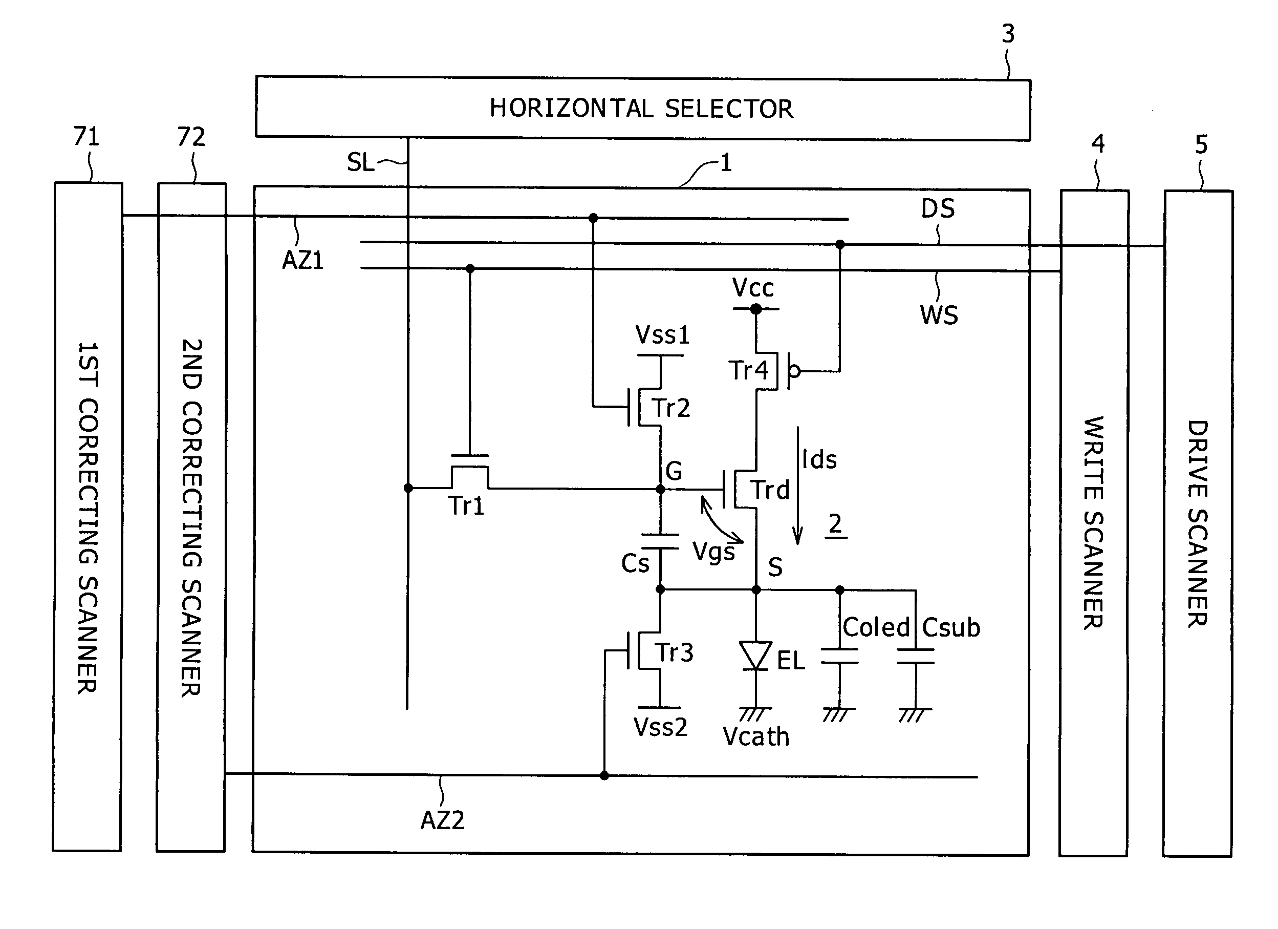
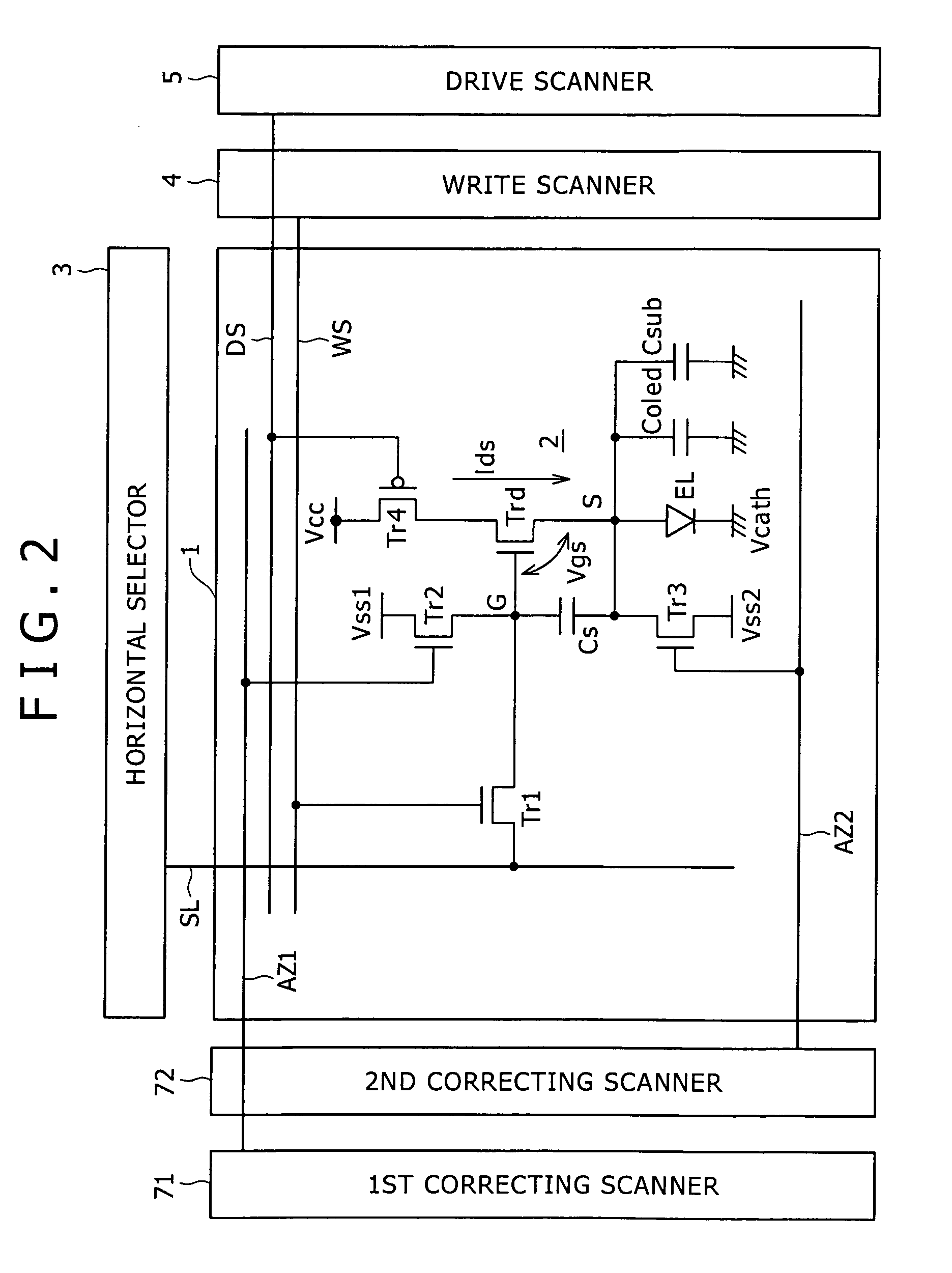
[0069]According to an embodiment of the present invention, the capacitance C used to correct the mobility is increased for making the mobility correction easy. The capacitance C may be increased by increasing the light-emitting device capacitance Coled or the pixel capacitance Cs or adding the additional capacitance Csub. The light-emitting device capacitance Coled is determined by the pixel size, the pixel aperture ratio, and the basic properties of the organic EL material of the light-emitting device, and hence it is difficult to increase simply. Increasing the pixel capacitance Cs results in an increase in the anode potential at the time the signal voltage is written. Specifically, the increase in the anode potential is determined by Cs / (Cs+Coled)×ΔV. Therefore, the input signal voltage gain represented by Coled / (Cs+Coled) is lowered. In order to make up for the reduction in the input signal voltage gain, the amplitude level of the video signal has to be increased, putting a burd...

third embodiment

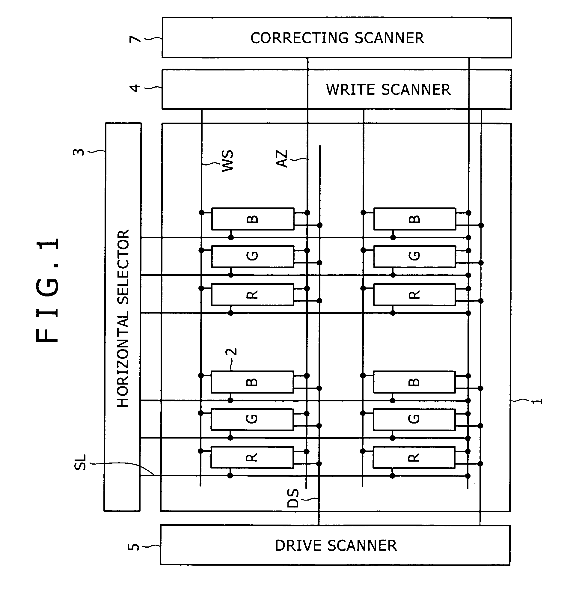
[0081]FIG. 14 is a fragmentary plan view of a display apparatus according to the present invention. FIG. 14 shows a set of red, green, and blue pixels. R, G, B pixel circuits 2 have a red light-emitting device, a green light-emitting device, and a blue light-emitting device, respectively. The additional capacitance Csub in each of the pixel circuits 2 has a capacitance value which is different for each light-emitting device, thereby making times requisite to operate respective correcting section in the R, G, B pixel circuits 2 uniform.

[0082]Generally, for producing R, G, B light-emitting devices, organic EL materials of which the light-emitting devices are to be made are coated differently for the colors R, G, B. Since the organic EL materials and their film thicknesses are different for the colors R, G, B, the light-emitting device capacitances Coled for the colors R, G, B are different from each other. If white organic EL light-emitting devices are colored with R, G, B filters and...


PUM


Abstract

Disclosed herein is a pixel circuit that includes a correcting section configured to correct the input voltage sampled in the pixel capacitance in order to cancel out the dependency of the output current on the carrier mobility. In the pixel circuit, the correcting section operates depending on the control signal supplied from the scanning line to extract the output current from the drive transistor and introduce the extracted output current into a capacitance of the light-emitting device and the pixel capacitance, thereby correcting the input voltage. The pixel circuit further includes an additional capacitance added to the capacitance of the light-emitting device. In the pixel circuit, a portion of the output current extracted from the drive transistor flows into the additional capacitance to give a time margin to operation of the correcting section.

Description

CROSS REFERENCES TO RELATED APPLICATIONS[0001]The present invention contains subject matter related to Japanese Patent Application JP 2005-294308 filed in the Japanese Patent Office on Oct. 7, 2005, the entire contents of which being incorporated herein by reference.BACKGROUND OF THE INVENTION[0002]1. Field of the Invention[0003]The present invention relates to a pixel circuit for current-driving light-emitting devices disposed at respective pixels. The present invention is also concerned with an active-matrix display apparatus having a matrix of such pixel circuits, for controlling currents supplied to light-emitting devices, such as organic EL devices, with insulated-gate field-effect transistors disposed in the respective pixel circuits.[0004]2. Description of the Related Art[0005]Image display apparatuses, such as liquid-crystal display apparatuses have a matrix of liquid-crystal pixels and control the intensity of light passing through or reflected by the pixels depending on im...

Claims


Application Information

Patent Timeline
Patent Type & Authority Patents(United States)
IPC IPC(8): G09G3/30H05B44/00
CPCG09G3/3233G09G2300/0417G09G2300/0819G09G2300/0842G09G2300/0852G09G2320/043G09G2310/0251G09G2310/0256G09G2310/0262G09G2320/0233G09G2300/0861
Inventor YAMASHITA, JUNICHIUCHINO, KATSUHIDE
Owner SONY CORP
Why Eureka
Try Eureka