Wafer level package and manufacturing method thereof

a technology of wafers and level packages, applied in the direction of semiconductor devices, semiconductor/solid-state device details, electrical devices, etc., can solve the problems of reducing the reliability of a device, increasing the size and the number of processes of a chip, and reducing the signal transmission speed, so as to improve the reliability of bonding

Inactive Publication Date: 2010-02-16
SAMSUNG ELECTRO MECHANICS CO LTD
View PDF7 Cites 25 Cited by
  • Summary
  • Abstract
  • Description
  • Claims
  • Application Information

AI Technical Summary

Benefits of technology

[0018]The present invention has been invented in order to overcome the above-described problems and it is, therefore, an object of the present invention to provide a wafer level package and a manufacturing method thereof capable of improving bonding reliability between an under bump metal and a bump by forming a buffer pattern separated through a trench on a center of the under bump metal used as a ball pad.

Problems solved by technology

However, the conventional wafer level package manufactured in a wafer level has disadvantages of increasing resistance by causing a crack of an interface between the ball pad unit 15 and the solder ball 17 when mounting the solder ball 17 and of reducing reliability of a device by causing an open phenomenon in case of excessive resistance.
However, there is a disadvantage of increasing a chip size and the number of processes by forming a multilayer solder ball.
Further, there is a disadvantage of reducing a signal transmission speed by increasing parasitic capacitance formed on a substrate, an insulation layer and a ball pad when increasing an area of the solder ball.

Method used


Image

  • Wafer level package and manufacturing method thereof
  • Wafer level package and manufacturing method thereof
  • Wafer level package and manufacturing method thereof

Examples


Embodiment Construction

[0033]Hereinafter, a matter regarding to a construction, a manufacturing method and an operation effect of a wafer level package in accordance with the present invention will be appreciated clearly through the following detailed description with reference to the accompanying drawings illustrating preferable embodiments of the present invention.

[0034]Hereinafter, a wafer level package and a manufacturing method thereof in accordance with one embodiment of the present invention will be described in detail with reference to the accompanying drawings.

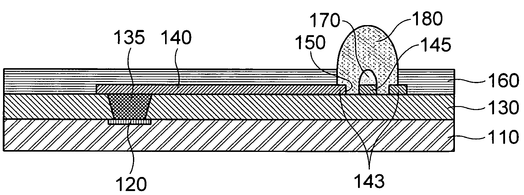
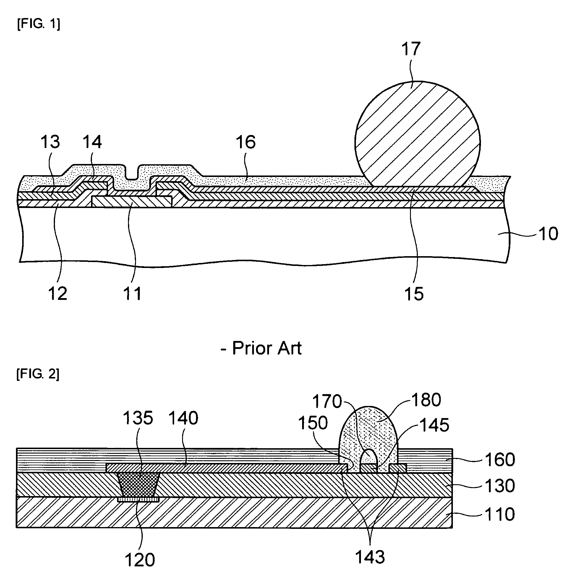
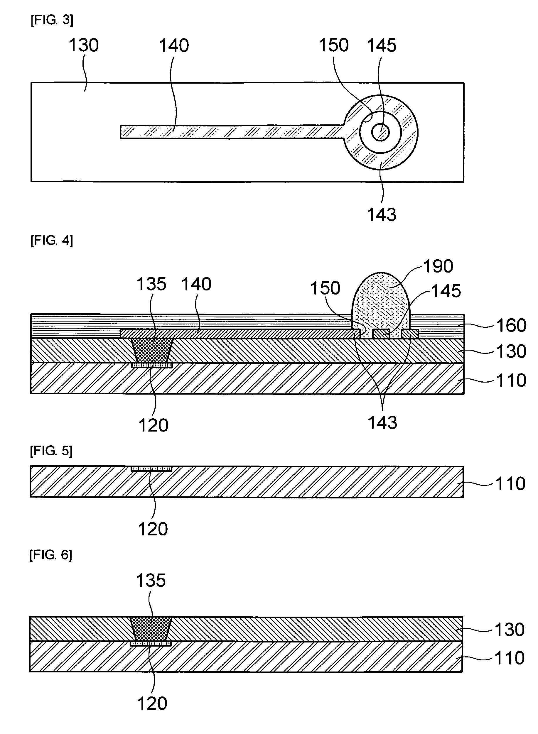
[0035]FIG. 2 is a cross sectional view showing a wafer level package in accordance with one embodiment of the present invention, FIG. 3 is a plan-view showing an under bump metal and a buffer pattern in FIG. 2 and FIG. 4 is a cross sectional view showing a wafer level package in accordance with a modified embodiment of the present invention.

[0036]First of all, as shown in FIG. 2, in accordance with one embodiment of the present invention, t...


PUM


Abstract

A wafer level package and a manufacturing method thereof capable of reducing stress between an under bump metal and a bump. The wafer level package includes a substrate provided with a plurality of chip pads on a top surface; a first passivation layer to expose the chip pads; vias connected to the chip pads by passing through the first passivation layer; a metal wiring layer formed on the first passivation layer and connected to the vias; an under bump metal formed on the first passivation layer to be connected to the metal wiring layer and having a buffer pattern separated through a trench on a center; a second passivation layer formed on the first passivation layer to expose the under bump metal; a first bump formed on the buffer pattern; and a second bump filling the trench and formed on the first bump and the under bump metal.

Description

CROSS-REFERENCE TO RELATED APPLICATIONS[0001]This application claims the benefit of Korean Patent Application No. 10-2008-0056817 filed with the Korea Intellectual Property Office on Jun. 17, 2008, the disclosure of which is incorporated herein by reference.BACKGROUND OF THE INVENTION[0002]1. Field of the Invention[0003]The present invention relates to a wafer level package and a manufacturing method thereof; and, more particularly, to a WLP (Wafer Level Package) capable of improving bonding reliability between an under bump metal and a bump formed on an upper part thereof by forming a buffer pattern on a central part of the under bump metal of a metal wiring layer through a trench and a manufacturing method thereof.[0004]2. Description of the Related Art[0005]As electronic appliances have become gradually smaller, lighter, high speed and high capacity, the development of a semiconductor package with a new structure has been needed so that the semiconductor package corresponds to th...

Claims


Application Information

Patent Timeline
Patent Type & Authority Patents(United States)
IPC IPC(8): H01L23/48H01L23/52H01L29/40
CPCH01L24/11H01L24/12H01L2224/0401H01L2224/0231H01L2224/13099H01L2224/13139H01L2224/16H01L2924/01013H01L2924/01029H01L2924/01047H01L2924/01075H01L2924/30105H01L2924/01005H01L2924/01006H01L2924/01033H01L2924/014H01L2224/0239H01L2924/351H01L2224/05147H01L2224/05124H01L2224/05551H01L2224/056H01L2224/05555H01L2224/02351H01L24/05H01L24/13H01L24/03H01L2924/0001H01L2224/05548H01L2224/13024H01L24/02H01L2924/00H01L2224/02H01L2924/00014H01L23/12H01L23/50
Inventor JEON, HYUNG JINYI, SUNGLEE, JONG YUNKWEON, YOUNG DOBAEK, JONG HWAN
Owner SAMSUNG ELECTRO MECHANICS CO LTD
Why Eureka
Try Eureka