
Memory circuits with reduced leakage power and design structures for same

a memory circuit and leakage power technology, applied in the field of electronic memory circuits, can solve the problems of substantial leakage power through the pull-down transistor of the register array cell, active power, and substantial leakage power, and achieve the effect of reducing leakage power

Active Publication Date: 2010-02-23
TWITTER INC
View PDF6 Cites 16 Cited by
  • Summary
  • Abstract
  • Description
  • Claims
  • Application Information

AI Technical Summary

Benefits of technology

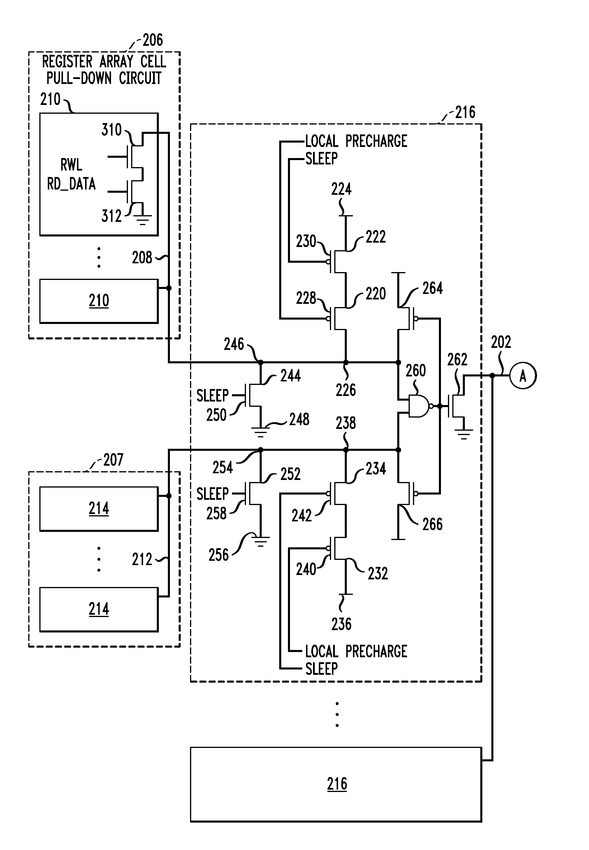
"The present invention provides techniques for reducing leakage power in electronic memory circuits, such as large register-file arrays. This is achieved by including a global read bit line, a global read bit line latch, and multiple sub-arrays. Each sub-array includes a local read bit line, a local write bit line, and a plurality of memory cells. The local read bit line is decoupled from the local write bit line. The invention also includes a local multiplexing block and a global multiplexing block for selectively interconnecting the read bit lines and maintaining the global read bit line in a discharged state. The invention may be realized in the form of an integrated circuit."

Problems solved by technology

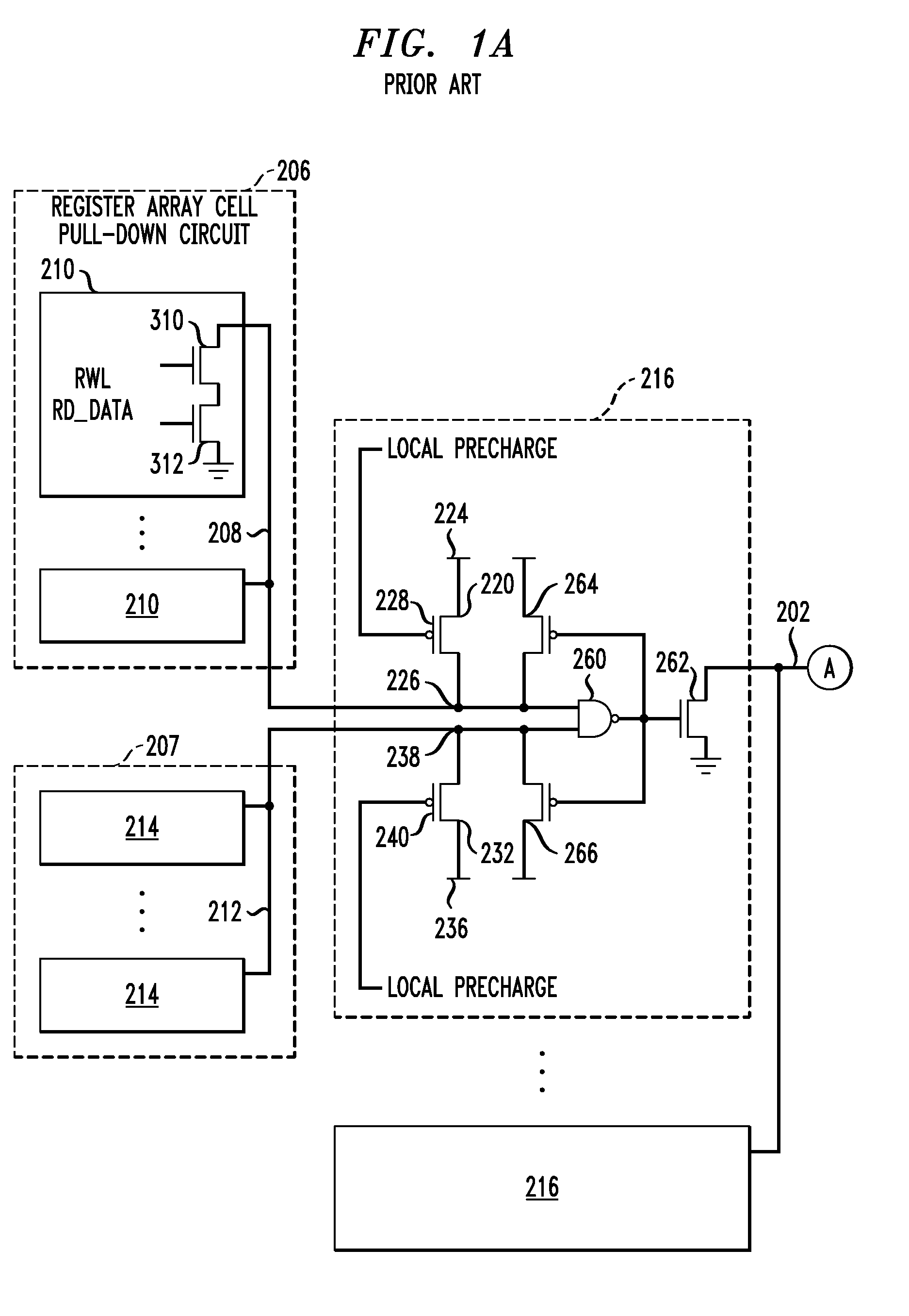
When there is no evaluate for a long time, then the dynamic bit lines stay in pre-charge; however, that also causes substantial leakage power through the register array cell's pull-down transistors (usually 8 or 16 cells dotted together—that is, the bit line for each cell is electrically connected).
Numerous techniques have been proposed to reduce the active power of dynamic READ, but in scenarios where the array will not be accessed for a long time, the leakage power can be substantial as well.

Method used


Image

  • Memory circuits with reduced leakage power and design structures for same
  • Memory circuits with reduced leakage power and design structures for same
  • Memory circuits with reduced leakage power and design structures for same

Examples


Embodiment Construction

[0015]Embodiments of the invention discharge the bit lines to ground, instead of keeping them in a pre-charged phase, thereby saving substantial stand-by power (leakage power) in, for example, dynamic register arrays. If and when a large dynamic register array is not required to be accessed for a long period of time, control logic issues a ‘SLEEP’ signal to the array, and that signal will substantially immediately cause discharge of all local bit lines (LBL) and all global bit lines (GBL) from their pre-charged states. The same SLEEP signal will also disable further pre-charging of local and global bit-lines. When the register array needs to be accessed again, the SLEEP signal will go low (that is, in the exemplary embodiment, assume a “low” or “zero” logical state) and one additional pre-charge-evaluate cycle will bring the array to a normal read mode.

[0016]One or more embodiments of this power-saving technique are advantageous when there is a need to shut-down a large dynamic regi...


PUM


Abstract

A memory circuit includes a global read bit line, a global read bit line latch, and a plurality of sub-arrays, each of which includes first and second local read bit lines, first and second local write bit lines, and first and second pluralities of memory cells interconnected, respectively, with the first and second local read bit lines and the first and second local write bit lines. The local read bit lines are decoupled from the local write bit lines. A local multiplexing block is interconnected with the first and second local read bit lines and is configured to ground the first and second local read bit lines upon assertion of a SLEEP signal, and to selectively interconnect the local read bit lines to the global read bit line. A global multiplexing block is interconnected with the global read bit line and is configured to maintain the global read bit line in a substantially discharged state upon assertion of the SLEEP signal and to interconnect the global read bit line to the global read bit line latch. Also included are design structures for circuits of the kind described.

Description

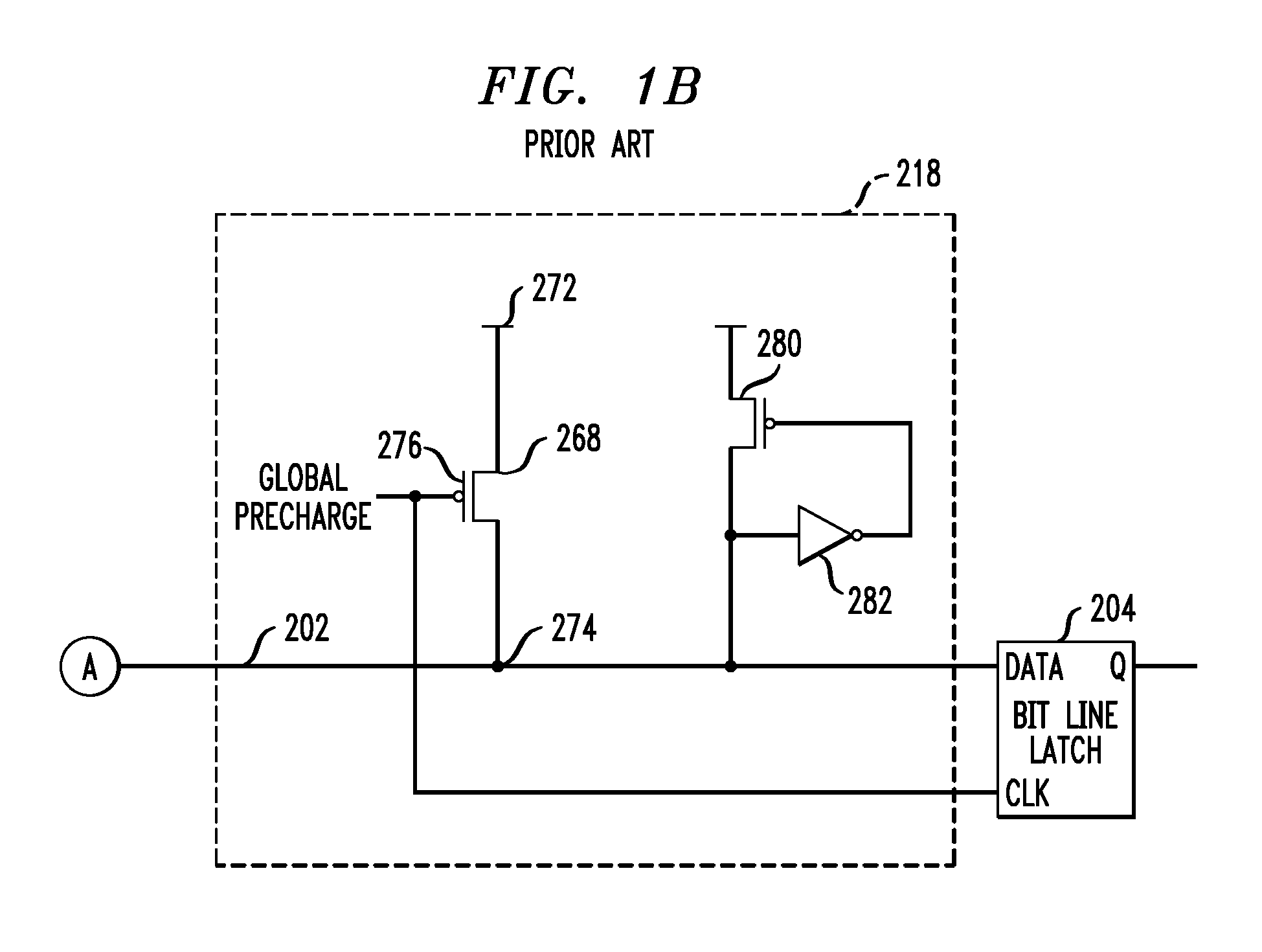
FIELD OF THE INVENTION[0001]The present invention generally relates to electronic circuitry, with associated design structures, and, more particularly, to electronic memory circuits, such as large register-file arrays, with associated design structures.BACKGROUND OF THE INVENTION[0002]Typical dynamic bit lines use a pre-charge phase, followed by the evaluate phase, in every cycle. This consumes substantial power, as usually the clock signal CLK acts as the pre-charge, and the clock signal is of course coming in every cycle. When there is no evaluate for a long time, then the dynamic bit lines stay in pre-charge; however, that also causes substantial leakage power through the register array cell's pull-down transistors (usually 8 or 16 cells dotted together—that is, the bit line for each cell is electrically connected). Numerous techniques have been proposed to reduce the active power of dynamic READ, but in scenarios where the array will not be accessed for a long time, the leakage ...

Claims


Application Information

Patent Timeline
Patent Type & Authority Patents(United States)
IPC IPC(8): G11C5/14
CPCG11C7/12G11C7/18G11C11/413G11C2207/2227
Inventor CHU, SAM GAT-SHANGISLAM, SAIFULKIM, JAE-JOONKOSONOCKY, STEPHEN V.
Owner TWITTER INC
Learn More