Nanowire-templated lateral epitaxial growth of non-polar group III nitrides

a technology of lateral epitaxial growth and nanowires, which is applied in the direction of crystal growth process, polycrystalline material growth, chemically reactive gas growth, etc., can solve the problems of both redshift of optical transition and reduction of oscillator strength

Active Publication Date: 2010-03-02
NAT TECH & ENG SOLUTIONS OF SANDIA LLC
View PDF17 Cites 27 Cited by
  • Summary
  • Abstract
  • Description
  • Claims
  • Application Information

AI Technical Summary

Problems solved by technology

However, the fields cause spatial separation of electrons and holes within quantum wells, w...

Method used


Image

  • Nanowire-templated lateral epitaxial growth of non-polar group III nitrides
  • Nanowire-templated lateral epitaxial growth of non-polar group III nitrides
  • Nanowire-templated lateral epitaxial growth of non-polar group III nitrides

Examples


Embodiment Construction

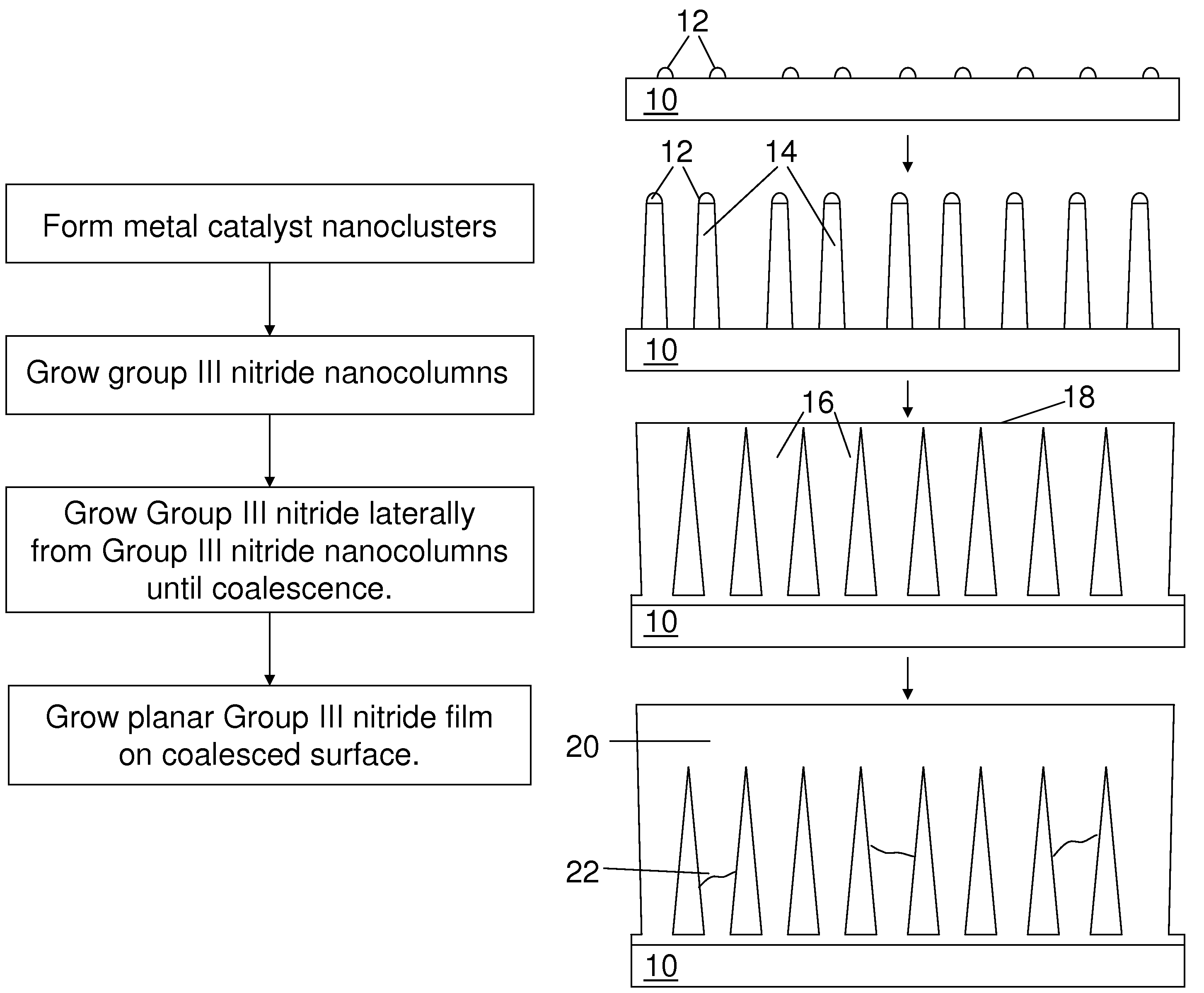
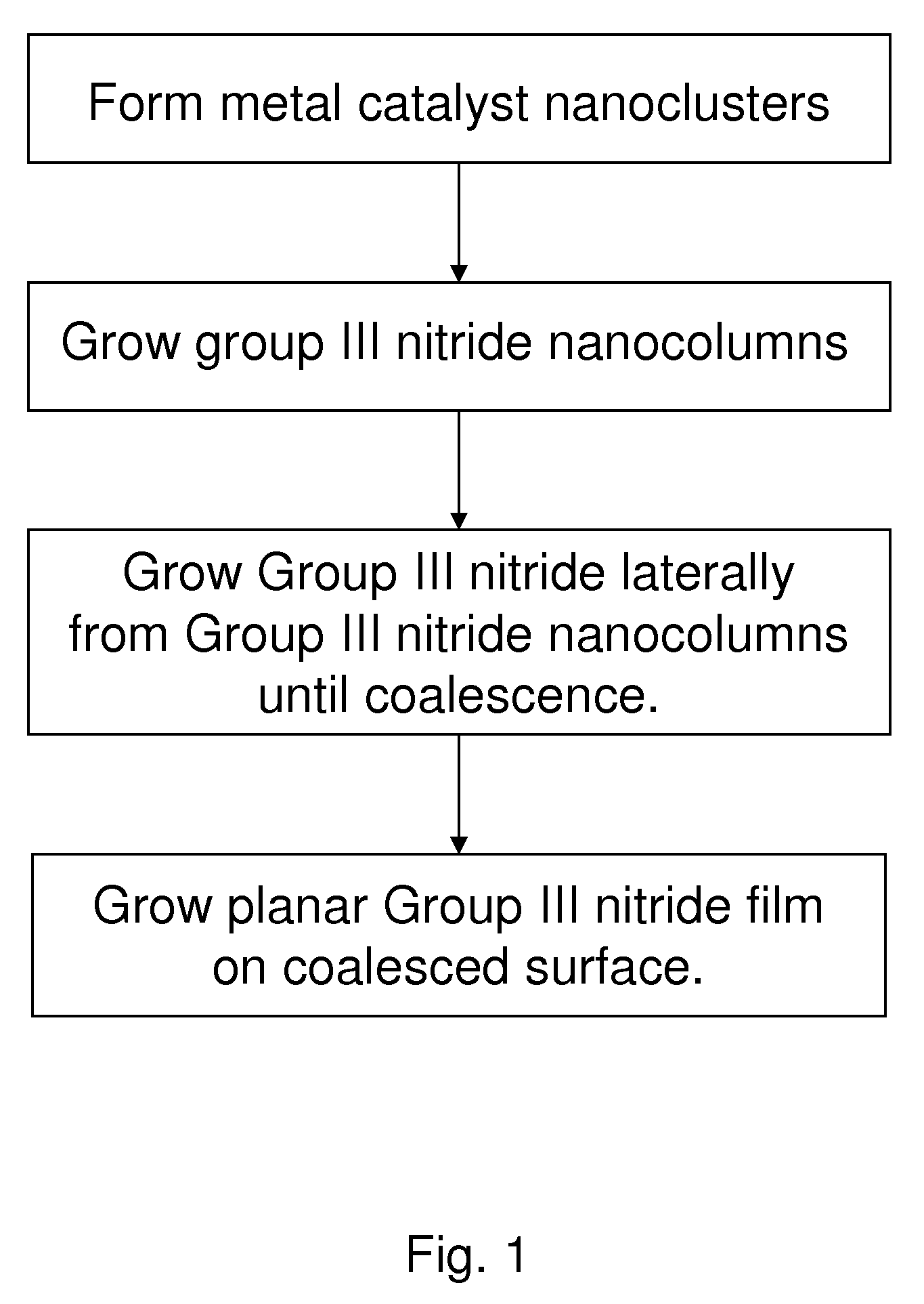
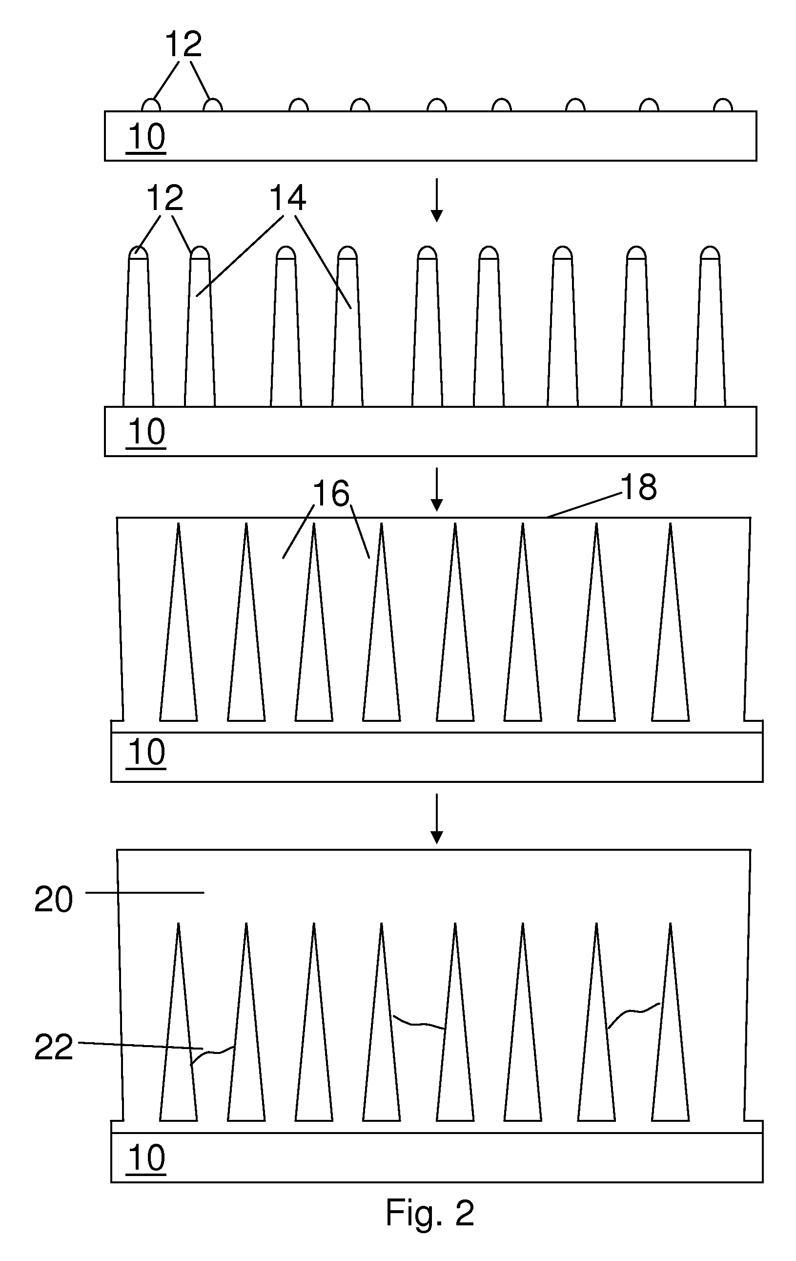
[0009]This invention comprises a method for growing high quality, nonpolar Group III nitrides using lateral growth from Group III nitride nanowires. The method of nanowire-templated lateral epitaxial growth (NTLEG) employs crystallographically aligned, substantially vertical Group III nitride nanowire arrays grown by metal-catalyzed metal-organic chemical vapor deposition (MOCVD) as templates for the lateral growth and coalescence of virtually crack-free Group III nitride films. This method requires no patterning or separate nitride growth step.

[0010]This invention comprises a method for growing virtually crack-free a-plane GaN on r-plane sapphire by using a mode of metal-organic chemical vapor deposition (MOCVD) that produces epitaxial lateral growth of Group III nitride material from the sidewalls of crystallographically oriented and substantially single-crystal Group III nitride nanowires or nanocolumns. A reduction in defects is made possible by minimizing the strain energy in t...


PUM


Abstract

A method for growing high quality, nonpolar Group III nitrides using lateral growth from Group III nitride nanowires. The method of nanowire-templated lateral epitaxial growth (NTLEG) employs crystallographically aligned, substantially vertical Group III nitride nanowire arrays grown by metal-catalyzed metal-organic chemical vapor deposition (MOCVD) as templates for the lateral growth and coalescence of virtually crack-free Group III nitride films. This method requires no patterning or separate nitride growth step.

Description

[0001]The United States Government has rights in this invention pursuant to Department of Energy Contract No. DE-AC04-94AL85000 with Sandia Corporation.CROSS-REFERENCE TO RELATED APPLICATIONS[0002]This application is related to a copending application, Highly Aligned Vertical GaN Nanowires Using Submonolayer Metal Catalysts,” application Ser. No. 11 / 866,684 filed Oct. 3, 2007, which has the same inventors.BACKGROUND OF THE INVENTION[0003]This invention relates to a method of growing high quality, nonpolar Group III nitrides. Group III nitrides that are conventionally grown on c-plane sapphire substrates have a c-plane surface, which is inherently polar due to the crystallographic location of the Group III atoms and nitrogen atoms in the (0001) plane (c-plane). The resulting internal electric fields are advantageous for applications where the formation of a two-dimensional electron gas is desired, as in transistors. However, the fields cause spatial separation of electrons and holes ...

Claims


Application Information

Patent Timeline
IPC IPC(8): H01L21/205C30B25/00C30B29/38C30B29/60
CPCC30B25/005C30B25/02C30B25/20C30B29/403H01L21/02389H01L21/0242H01L21/02433H01L21/02458H01L21/0254H01L21/02603H01L21/0262H01L21/02645H01L21/02647H01L21/02653Y10S977/891Y10S977/817Y10S117/902Y10S977/821Y10S977/816Y10S977/762
Inventor WANG, GEORGE T.LI, QIMINGCREIGHTON, J. RANDALL
Owner NAT TECH & ENG SOLUTIONS OF SANDIA LLC
Why Eureka
Try Eureka