Lattice-matched AllnN/GaN for optoelectronic devices

a technology of optoelectronic devices and allnn/gan, which is applied in the direction of semiconductor lasers, polycrystalline material growth, crystal growth process, etc., can solve the problems of no longer lattice-matched dbrs, dbrs are subject to the same issue, and may cause strain relaxation problems

Inactive Publication Date: 2007-01-04
ECOLE POLYTECHNIQUE FEDERALE DE LAUSANNE (EPFL)
View PDF1 Cites 26 Cited by
  • Summary
  • Abstract
  • Description
  • Claims
  • Application Information

AI Technical Summary

Problems solved by technology

Distributed Bragg reflectors (DBRs) are subject to the same issue.
As a result, GaN / GaInN multi-quantum-well (MQW) active layers grown on top of such DBRs are no longer lattice-matched, and strain relaxation issues may arise in the active zone.
As yet, AlInN has found little use in optoelectronic devices mainly because growth is difficult due to phase separation.

Method used


Image

  • Lattice-matched AllnN/GaN for optoelectronic devices
  • Lattice-matched AllnN/GaN for optoelectronic devices
  • Lattice-matched AllnN/GaN for optoelectronic devices

Examples


Embodiment Construction

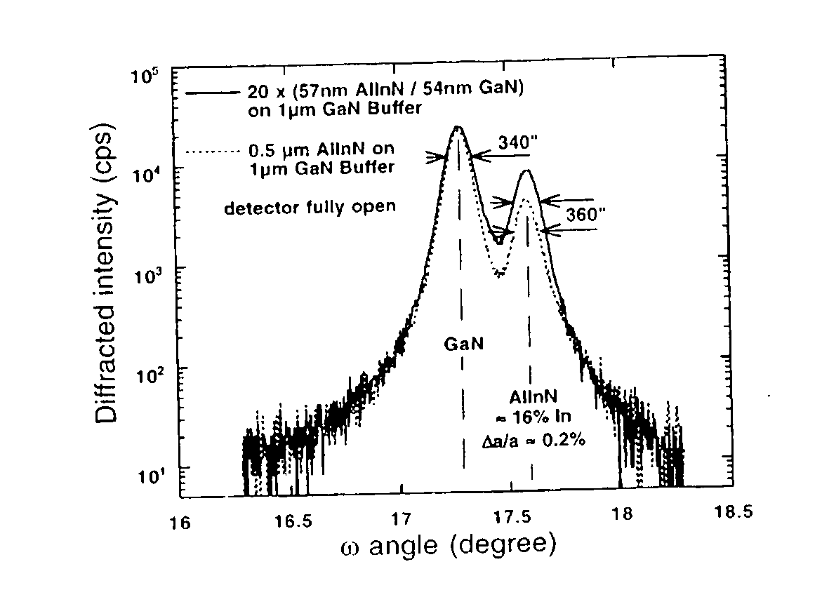
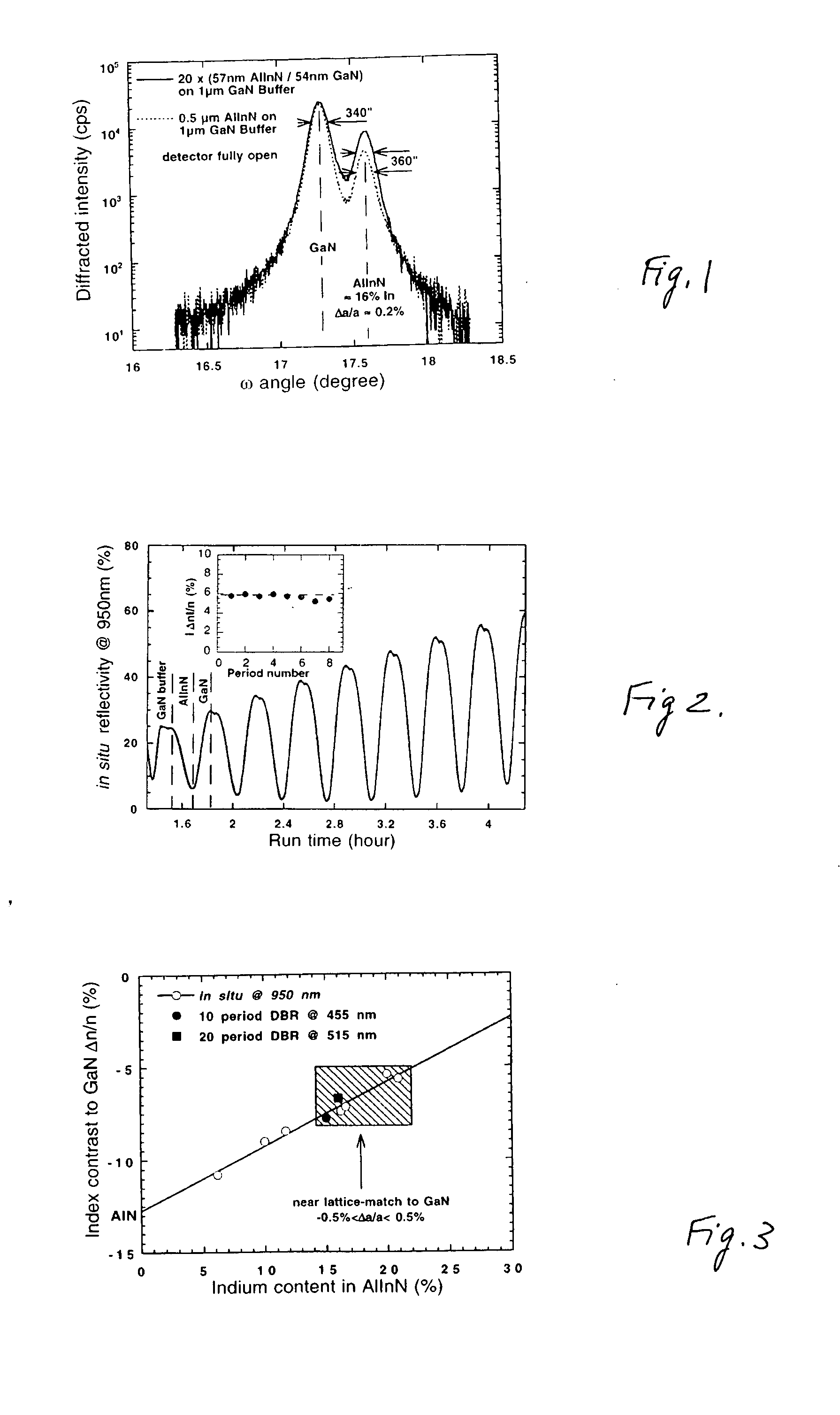
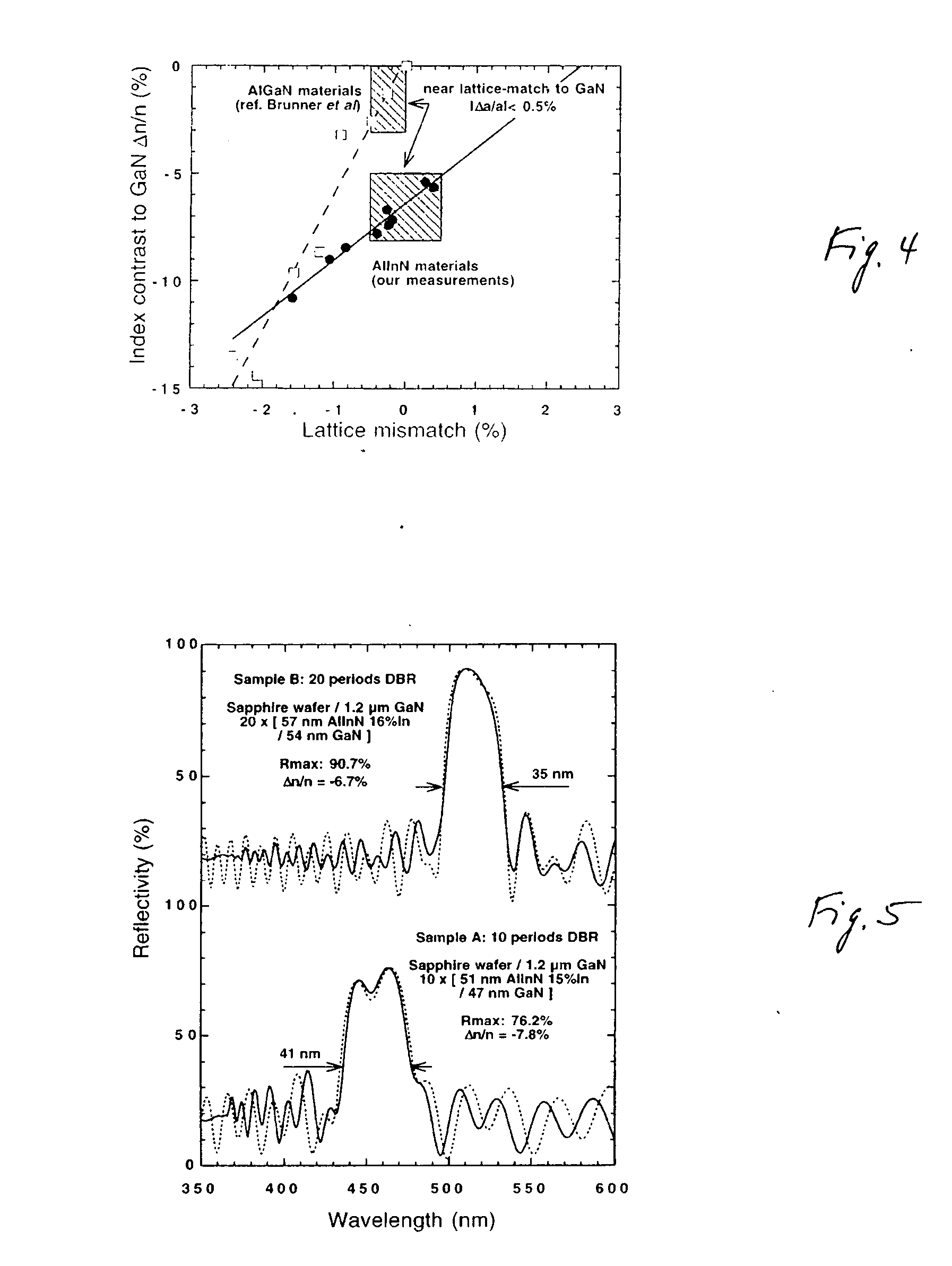
[0010] Growth has been achieved of Al0.84In0.16N / GaN DBRs near lattice-matched to GaN. Such DBRs are optically equivalent to state-of-the art Al0.6Ga0.4N / GaN mirrors and avoid the issues related to strain. Layers were grown in an AIXTRON 200 / 4 RF-S metalorganic vapor phase epitaxy system, on 2-inch c-plane sapphire substrates. The growth was initiated by a low-temperature GaN nucleation layer followed by a 1 μm thick GaN buffer layer. AlInN was deposited between 800° C. and 850° C. and at 50 to 75 mbar pressure using N2 carrier gas. Lower growth temperatures led to lower crystalline quality as revealed by high resolution X-ray diffraction (HRXD) (0002) scans. Higher growth temperatures resulted in decreased indium incorporation so that near-lattice matched alloys could no longer be obtained. Deposition rates ranged between 0.6 and 0.2 μm / h. During the DBR runs, growth was interrupted at each interface. GaN was deposited at 1050° C. using H2 and N2 carrier gas.

[0011] No degradation ...


PUM

PropertyMeasurementUnit
wavelengthaaaaaaaaaa
pressureaaaaaaaaaa
temperatureaaaaaaaaaa

Abstract

High-quality Al1-xInxN layers and AlInN / GaN Bragg mirrors near lattice-matched to GaN layers are grown by metalorganic vapor-phase epitaxy on a GaN buffer layer with no cracks over full 2-inch sapphire wafers. The index contrast relative to GaN is 6.5% to 11% for wavelengths ranging from 950 nm to 380 nm. A crack-free, 20 pairs Al0.84In0.16N / GaN distributed Bragg reflector is grown, centered at 515 nm with over 90% reflectivity and a 35 nm stopband. High-quality AlInN lattice matched to GaN can be used in GaN-based optoelectronics, for waveguides and for mirror structures in resonant-cavity light-emitting diodes and monolithic Fabry-Pérot cavities, for example.

Description

FIELD OF THE INVENTION [0001] The invention is concerned with Group III-Nitride optoelectronic devices which, more particularly, include a Bragg reflector element or an in-plane waveguide. BACKGROUND OF THE INVENTION [0002] AlInN materials hold great potential for GaN-based optoelectronics. Alloys with indium content between 14% and 22%, which are within a ±0.5% lattice mismatch to GaN, would be of special interest if they prove to exhibit a sufficiently high bandgap and refractive index contrast with GaN. Indeed. AlGaN is presently the standard material for optical engineering of GaN-based devices, but the requirement of achieving a high index contrast while at the same time avoiding the generation of cracks due to the lattice mismatch to GaN are opposites. As a consequence, for nitride-based laser diodes, AlGaN waveguide cladding layers are used with hardly more than 10% Al content (having 0.25% lattice mismatch) and an index contrast that does not exceed 2%. [0003] Distributed Br...

Claims


Application Information

Patent Timeline
Patent Type & Authority Applications(United States)
IPC IPC(8): B05D1/36
CPCB82Y20/00C30B25/02C30B29/40H01L21/0242H01L21/02458H01S2304/04H01L33/105H01S5/183H01S5/2004H01S5/32341H01S5/34H01L21/0254
Inventor CARLIN, JEAN-FRANCOISILEGEMS, MARC
Owner ECOLE POLYTECHNIQUE FEDERALE DE LAUSANNE (EPFL)
Why Eureka
Try Eureka