Base substrate for chip scale packaging

a technology of chip scale and base substrate, which is applied in the direction of semiconductor/solid-state device details, electrical equipment, semiconductor devices, etc., can solve the problems of etching methods that are expensive and time-consuming, and the packaging mentioned above has a chief defect, so as to achieve low cost and time-saving

Inactive Publication Date: 2010-03-09
SUBTRON TECH
View PDF5 Cites 0 Cited by
  • Summary
  • Abstract
  • Description
  • Claims
  • Application Information

AI Technical Summary

Benefits of technology

[0008]Accordingly, an object of the present invention is to provide a base substrate which can sufficiently meet the demands for miniaturizing and thinning the chip packaging, and which, at the same time, can be manufactured by a low cost and time-saving way.
[0009]An other object of the present invention is to provide an improved base substrate which can effectively improve the electrical performance of a chip attached thereon.

Problems solved by technology

The packaging mentioned above has a chief defect.
The vias and openings are formed generally by etching methods which are expensive and time-consuming.

Method used


Image

  • Base substrate for chip scale packaging
  • Base substrate for chip scale packaging
  • Base substrate for chip scale packaging

Examples


Embodiment Construction

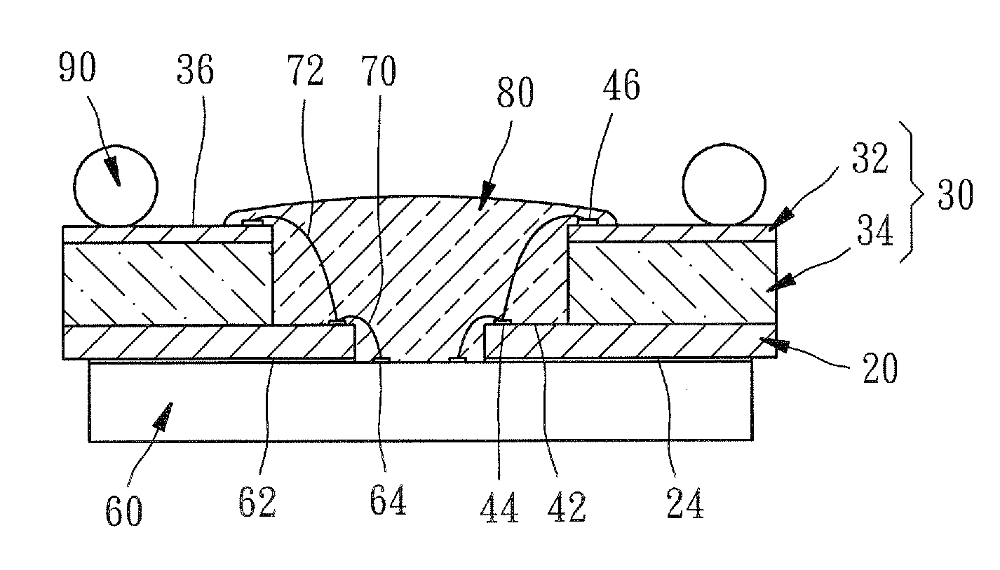
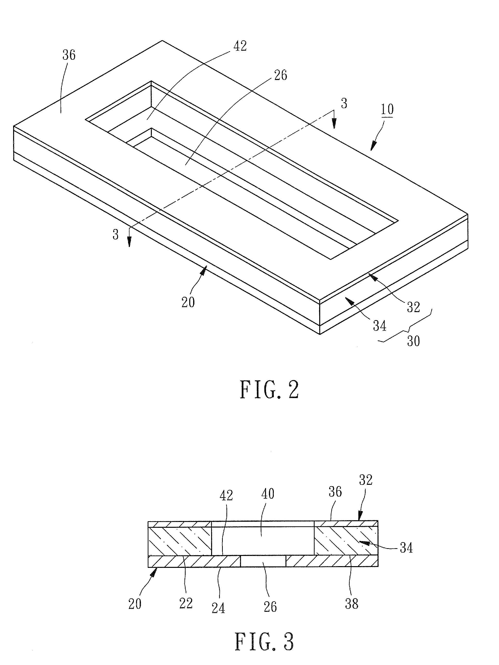
[0018]Referring firstly to FIGS. 2 and 3, the drawings illustrate a preferred embodiment of a base substrate according to one aspect of the present invention. In the drawings, reference numeral 10 denotes a base substrate, and the base substrate 10 comprises a carrier member 20 and an active member 30.

[0019]The carrier member 20 is made of an electrical conductive metal sheet, such as copper, iron, alloy of copper or any other suitable metal sheets. In this embodiment, the carrier member 20 is made of copper sheet with a predetermined thickness for providing sufficient supporting strength. The carrier member 20 has an upper surface 22, a bottom surface 24 and at least a first elongate through opening 26.

[0020]The active member 30 includes a base layer 32 and an intermediate layer 34 attached to the base layer 32. The base layer 32 is also made of an electrical conductive metal sheet, such as copper, iron, alloy of copper or any other suitable metal sheets, but thinner than the carri...


PUM


Abstract

A base substrate for chip scale package includes a carrier member made of electrical conductive metals with a first through opening; an active member laminated by a base layer made of electrical conductive metal and an intermediate layer made of electrical insulating or dielectric material, the active member having a through opening with a diameter larger that the diameter of the through opening of the base metal member; the active member being coupled with the carrier member in such a way that the intermediate layer is adhered to an upper surface of the carrier member, and these through openings are aligned to define a shoulder around the through opening of the base metal plate.

Description

BACKGROUND OF THE INVENTION[0001]1. Field of the Invention[0002]The present invention is generally related to chip assembly and packaging, and more particularly, to a base substrate for chip scale packaging.[0003]2. Description of the Related Art[0004]The conventional chip scale packaging, as shown in FIG. 1, generally has a base board 1 made of glass fibers mixed with epoxy resin. Base board 1 has a center through opening 2 and an upper circuit side 3 with a plurality of bond pads 4. A chip 5 has an active side 7 attached to a bottom side 6 of base board 1. Active side 7 of chip 5 has a plurality of bond pads 8 disposed on the centre portion thereof. Bond pads 8 are interconnected to bond pads 4 via connecting bond wires 9 passing though opening 2.[0005]The packaging mentioned above has a chief defect. It is that for being made of hard materials, base board 1 is always deformed or destroyed during punching or drilling used to form through opening 2.[0006]To eliminate this defect, U...

Claims


Application Information

Patent Timeline
Patent Type & Authority Patents(United States)
IPC IPC(8): H01L23/48
CPCH01L23/13H01L23/49816H01L24/49H01L23/3114H01L23/3128H01L2224/32014H01L2224/48091H01L2224/4824H01L2224/4911H01L2224/49175H01L2924/01029H01L2924/15311H01L2924/19107H01L2924/00014H01L24/48H01L2924/01033H01L2924/014H01L2224/32225H01L2224/73215H01L2924/00H01L2924/18165H01L2224/05554H01L2224/45099H01L2224/05599
Inventor BIAR, JEFFHUANG, CHIH-KUNG
Owner SUBTRON TECH
Why Eureka
Try Eureka