

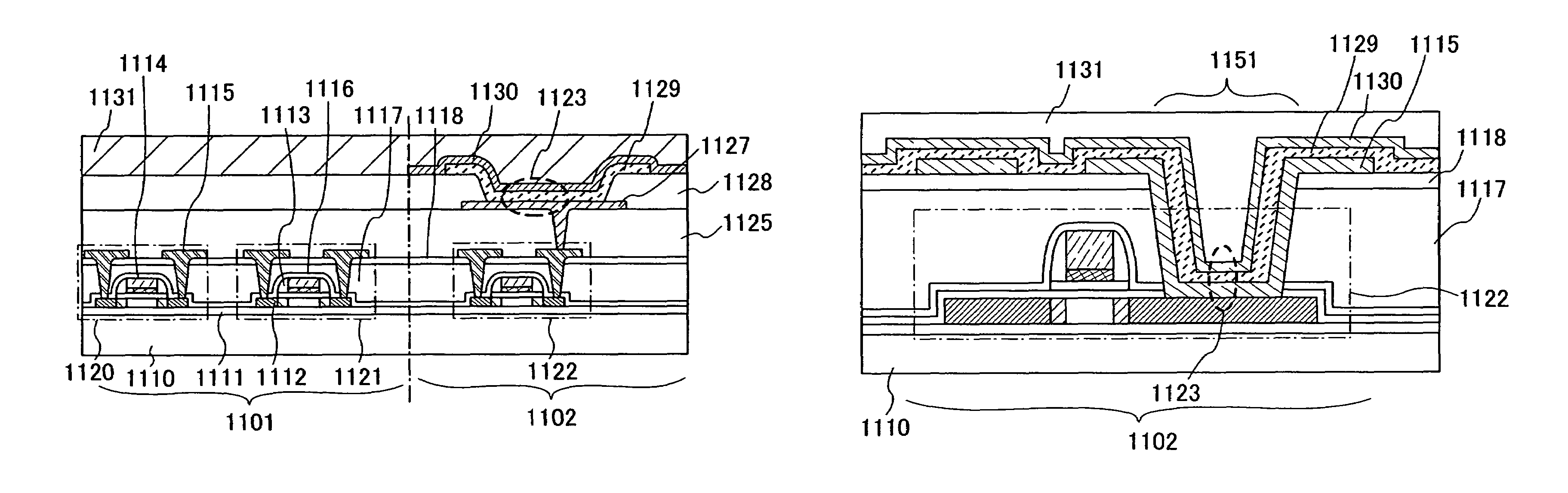
Semiconductor device
a semiconductor device and wireless communication technology, applied in semiconductor devices, digital storage, instruments, etc., can solve the problems of increasing the current consumption of the semiconductor device as a whole, reading other unnecessary information, amplifying an enormous amount of current, etc., and achieves low power consumption and low cost. , the effect of low cos
- Summary
- Abstract
- Description
- Claims
- Application Information
AI Technical Summary
Benefits of technology
Problems solved by technology
Method used
Image

Examples
embodiment mode 1
(Embodiment Mode 1)
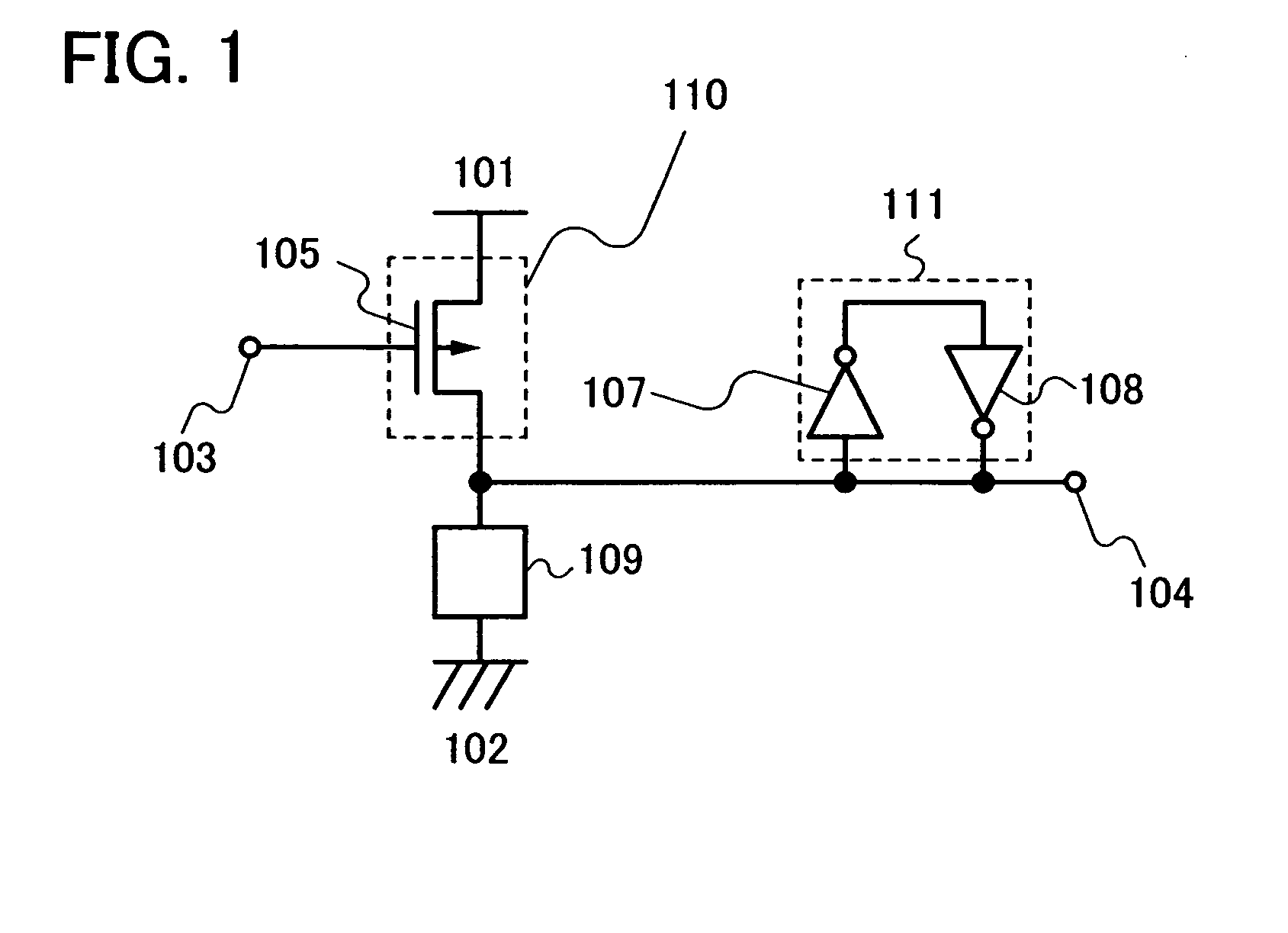
[0043]A first embodiment mode of a wireless chip according to the present invention is described with reference to FIG. 1. FIG. 1 shows a circuit diagram of a storage element of a nonvolatile storage device that is mounted to the wireless chip according to the present invention.
[0044]In FIG. 1, reference numerals 101, 102, 103, 104, 105, 107, 108, and 109 denote a power supply terminal, a ground terminal, a reset terminal, an output terminal, a P-type transistor, a first inverter, a second inverter, and an electronic element, respectively. The P-type transistor 105 forms the reset element 110. A source terminal, a drain terminal and a gate terminal of the P-type transistor 105 are connected to the power supply terminal 101, the output terminal 104, and the reset terminal 103, respectively. Also, the first inverter 107 and the second inverter 108 form a latch element 111.
[0045]As the electrical element, an electrical resistor for which electrical insulation is poss...
embodiment mode 2
(Embodiment Mode 2)
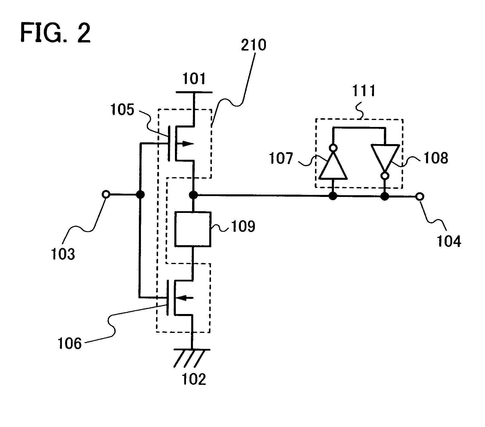
[0051]As a second embodiment mode of a wireless chip according to the present invention, a wireless chip with a structure different from that of the first embodiment mode is described with reference to FIG. 2. FIG. 2 is a circuit diagram of a storage element of a nonvolatile storage device that is mounted to the wireless chip according to the present invention.
[0052]FIG. 2 includes the power supply terminal 101, the ground terminal 102, the reset terminal 103, the output terminal 104, the P-type transistor 105, an N-type transistor 106, the first inverter 107, the second inverter 108, and the electrical element 109. The P-type transistor 105 and the N-type transistor 106 form a reset element 210. The source terminal, the drain terminal, and the gate terminal of the P-type transistor 105 are connected to the power supply terminal 101, the output terminal 104, and the reset terminal 103, respectively. A source terminal and a gate terminal of the N-type transistor 10...
embodiment 1
[0061]In this embodiment, an example of an electrical element that forms a nonvolatile storage device that is mounted to the wireless chip according to the present invention shown in Embodiment Mode 1 and Embodiment Mode 2 is described with reference to FIGS. 3A to 3C.
[0062]FIG. 3A is an example of forming an electrical element using an electrical resistor 301. A first terminal 302 and a second terminal 303 are electrically connected to the output terminal 104, and the ground terminal 102 of FIG. 1 described in Embodiment Mode 1, respectively. Also, the first terminal 302 and the second terminal 303 are electrically connected to the output terminal 104 and the N-type transistor 106 of FIG. 2 described in Embodiment Mode 2, respectively.
[0063]The electrical resistor 301 makes possible an electrical insulation by providing a region that is to be mechanically cut by laser drawing, and cutting this region by laser drawing. Also, the electrical resistor 301 makes possible an electrical i...
PUM
 Abstract
Description
Claims
Application Information