

Method for fabricating semiconductor device
a semiconductor and device technology, applied in the field of semiconductor device fabrication, can solve the problems of difficult height difference between active region and field region, and the inability to perform lpc opening process and gap filling process,
- Summary
- Abstract
- Description
- Claims
- Application Information
AI Technical Summary
Benefits of technology
Problems solved by technology
Method used
Image

Examples
Embodiment Construction
[0022]Hereinafter, detailed descriptions on certain embodiments of the present invention will be provided with reference to the accompanying drawings.
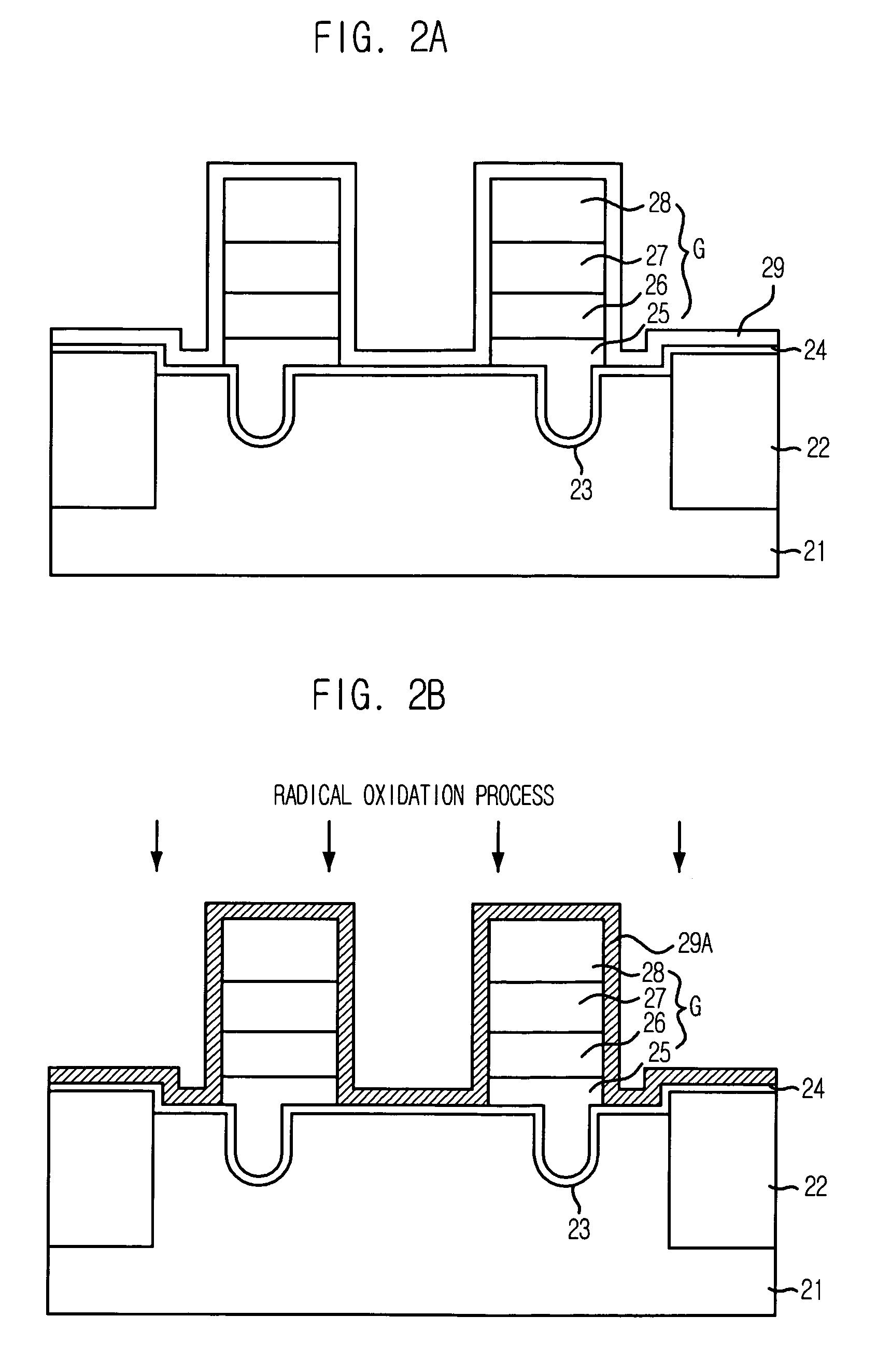
[0023]FIGS. 2A to 2C are cross-sectional views illustrating a method for fabricating a semiconductor device in accordance with an embodiment of the present invention.
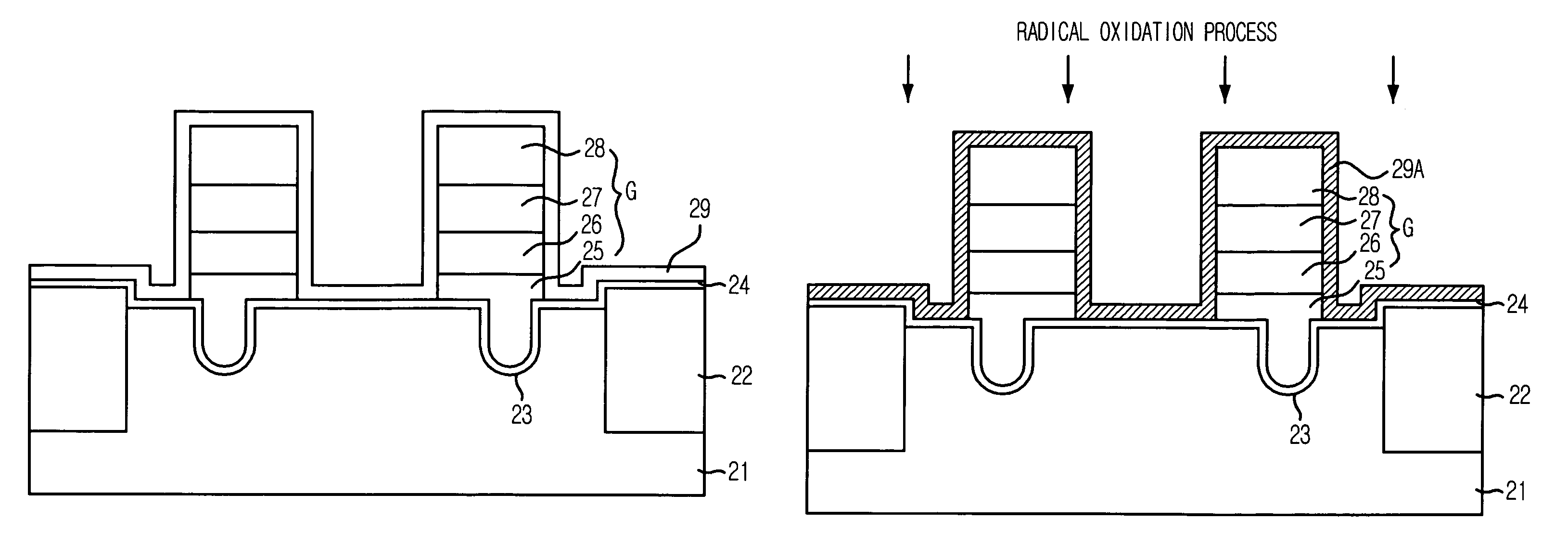
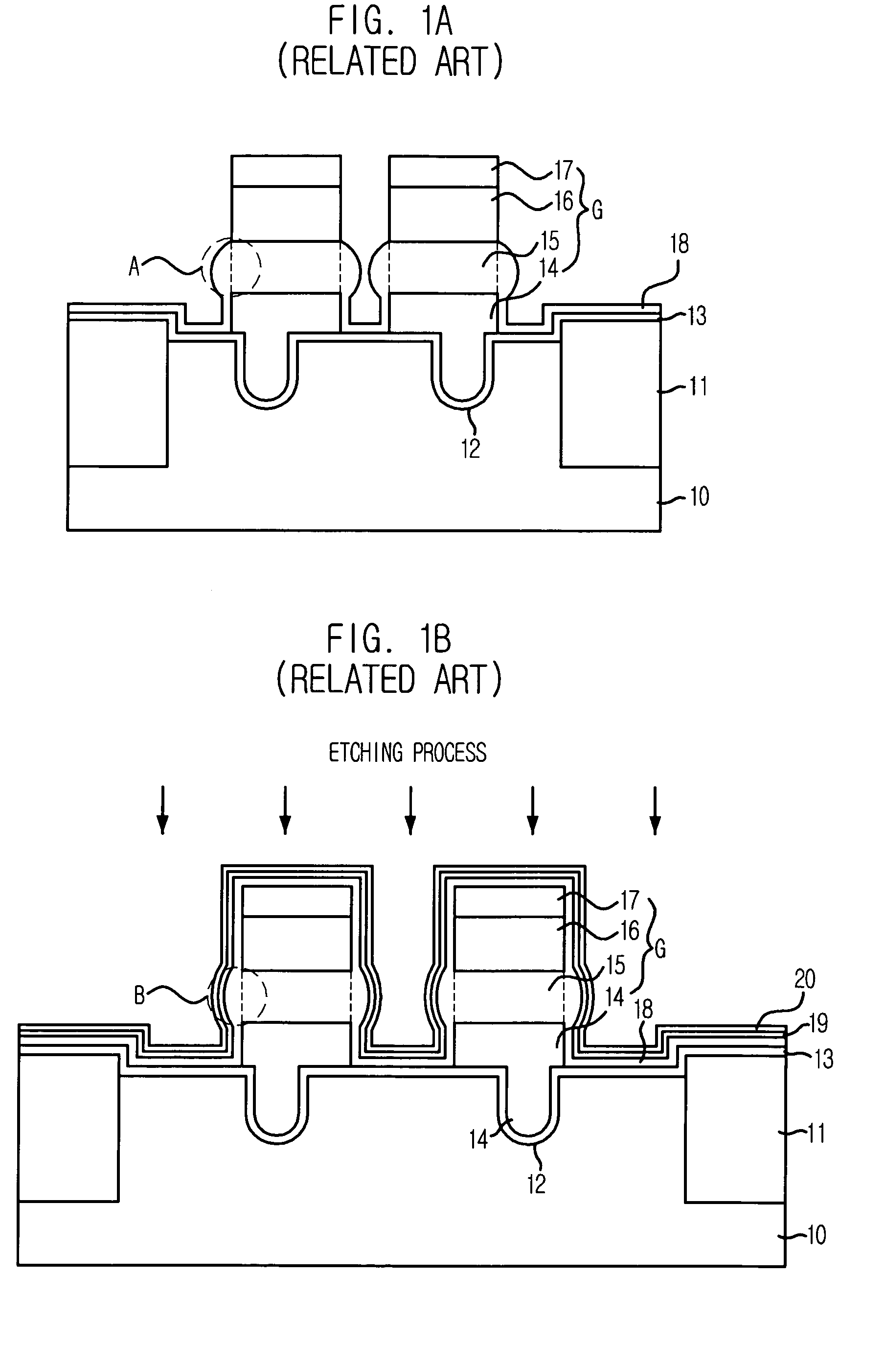
[0024]As shown in FIG. 2A, a plurality of device isolation layers 22 are formed in certain portions of a substrate 21 through a shallow trench isolation (STI) process. Then, a plurality of recesses 23 are formed in predetermined portions of the substrate 21.
[0025]A gate insulation layer 24 is formed over the above resulting structure and afterwards, a plurality of recess gate lines G are formed over the gate insulation layer 24 being partially filled into the recesses 23. Each of the recess gate lines G is formed by sequentially stacking the gate insulation layer 24, a polysilicon layer 25, a tungsten silicide layer 26, a gate hard mask 27, and an anti-reflective coating l...
PUM
| Property | Measurement | Unit |
|---|---|---|
| temperature | aaaaa | aaaaa |
| temperature | aaaaa | aaaaa |
| pressure | aaaaa | aaaaa |
Abstract
Description
Claims
Application Information