Low wet etch rate silicon nitride film

a silicon nitride film, low wet etching technology, applied in vacuum evaporation coating, coating, plasma technique, etc., can solve the problems of reducing the utility of etching stop, reducing the energy required to activate chemical reaction, and higher etching rate, so as to reduce the deposition temperature and high quality

Inactive Publication Date: 2010-03-16
APPLIED MATERIALS INC
View PDF154 Cites 377 Cited by
  • Summary
  • Abstract
  • Description
  • Claims
  • Application Information

AI Technical Summary

Benefits of technology

[0009]In contrast to traditional HDP gapfill deposition processes, some embodiments of the invention apply little or no RF bias power during the deposition process and provide a deposition to sputter ratio during film growth that is greater than or equal to 50:1, 75:1 or 100:1 in different embodiments. Also, in some embodiments a flow of argon gas is introduced into the processing chamber during deposition to assist in the formation of the high density plasma. The ratio of atomic-nitrogen flow to the atomic-argon flow may be maintained between 15:1 and 15:2 and the RF power applied to create the high density plasma may be between 5 and 15 watts per square centimeter.

Problems solved by technology

The high reactivity of the species in the plasma reduces the energy required to activate a chemical reaction.
The presence of impurities within a silicon nitride film often correlates with a higher etch rate and decreased utility as an etch stop.
Growing silicon nitride with conventional thermal CVD methods has succeeded in reducing the hydrogen content to below ten percent, however, the substrate temperatures for chemical vapor deposition are in the range of 700° C. to 1000° C. The higher temperatures can degrade and even ruin material properties and devices built in earlier processing steps.

Method used


Image

  • Low wet etch rate silicon nitride film
  • Low wet etch rate silicon nitride film
  • Low wet etch rate silicon nitride film

Examples


Embodiment Construction

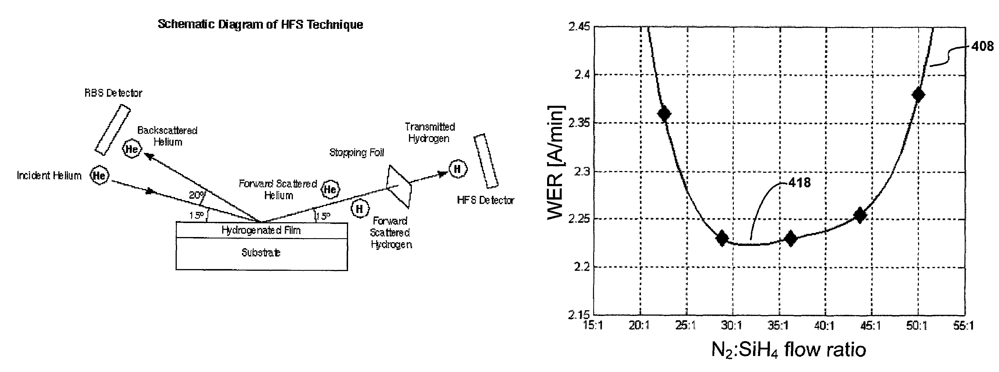
[0018]The present invention relates to methods of forming high quality silicon nitride films deposited using high density plasma CVD techniques. The high quality films exhibit low WERs compared to silicon oxide when both are exposed to the same etching agent. The low WER is achieved by a reduction in hydrogen content. The hydrogen content in the silicon nitride films may be below 10% or may be below 7% in different embodiments. The low hydrogen content of silicon nitride films deposited according to techniques of the invention can be achieved while the substrate is maintained at a relatively low temperature (<600° C.) during deposition.

[0019]Many applications which benefit from a silicon nitride film with a high density, low wet (or dry) oxide etch rate, high dielectric constant, high optical index of refraction, and other related physical properties would benefit from the use of embodiments of the present invention.

[0020]A significant impurity in prior art CVD silicon nitride films...


PUM

PropertyMeasurementUnit
temperatureaaaaaaaaaa
mean pressureaaaaaaaaaa

Abstract

The present invention pertains to methods of depositing low wet etch rate silicon nitride films on substrates using high-density plasma chemical vapor deposition techniques at substrate temperatures below 600° C. The method additionally involves the maintenance of a relatively high ratio of nitrogen to silicon in the plasma and a low process pressure.

Description

BACKGROUND OF THE INVENTION[0001]The present invention relates to nano-manufacturing technology solutions involving equipment, processes, and materials used in the deposition, patterning, and treatment of thin-films and coatings, with representative examples including (but not limited to) applications involving: semiconductor and dielectric materials and devices, silicon-based wafers, flat panel displays (such as TFTs), masks and filters, energy conversion and storage (such as photovoltaic cells, fuel cells, and batteries), solid state lighting (such as LEDs and OLEDs), magnetic and optical storage, micro-electro-mechanical systems (MEMS) and nano-electro-mechanical systems (NEMS), micro-optic and optoelectronic devices, architectural and automotive glasses, metallization systems for metal and polymer foils and packaging, and micro- and nano-molding. More particularly, the invention relates to the application of thin films onto a surface. Even more particularly, the invention relate...

Claims


Application Information

Patent Timeline
Patent Type & Authority Patents(United States)
IPC IPC(8): H01L21/00C23C14/08
CPCC23C16/345C23C16/505H01L21/31111H01L21/3185H01L21/0217H01L21/02211H01L21/02274
Inventor MUNGEKAR, HEMANT P.WU, JINGLEE, YOUNG S.WANG, ANCHUAN
Owner APPLIED MATERIALS INC
Why Eureka
Try Eureka