Semiconductor device and programming method therefor

a technology of semiconductor devices and data reading methods, which is applied in the direction of semiconductor devices, semiconductor/solid-state device details, electrical apparatus, etc., can solve the problems of large scale of programming circuits relative to memory capacity, reduced yield, and inability to retain device id or trimming data, etc., to achieve advantageously preserve semiconductor die space, the effect of increasing the number of steps

Inactive Publication Date: 2010-03-16
MONTEREY RES LLC
View PDF12 Cites 2 Cited by
  • Summary
  • Abstract
  • Description
  • Claims
  • Application Information

AI Technical Summary

Benefits of technology

[0011]According to an aspect of the present invention, preferably, there is provided a semiconductor device including a pair of metal interconnections provided above a semiconductor substrate, a program layer provided over the pair of metal interconnections and in which an opening may be selectively formed in the program layer on the basis of programming information, and a read circuit reading the programming information by determining whether such an opening is formed in the program layer by utilizing an electrostatic capacitance between the pair of metal interconnections. In accordance with the present invention, the information can be retained even if there is an opening in the program layer. Accordingly, the trimming information, the device ID information, and / or the like can be stored in a logic device that does not have a memory transistor. Unlike a CAM cell, a memory transistor does not have to be included and the number of steps is not increased during wafer processing. In addition, there is no need for a read circuit, advantageously preserving semiconductor die space. Further, the semiconductor device employed in the present invention has a higher reliability than that having a fuse.
[0013]According to another aspect of the present invention, preferably, there is provided a data reading method including the steps of applying a voltage across a pair of metal interconnections provided below a program layer in which an opening may be selectively formed on the basis of programming information and reading the programming information by determining whether such an opening is formed in the program layer by utilizing an electrostatic capacitance between the pair of metal interconnections. In accordance with the present invention, the information can be retained even if there is an opening in the program layer. Accordingly, the trimming information, the device ID information, or the like can be stored in a logic device that does not have a memory transistor. Unlike the CAM cell, the memory transistor does not have to be included and the number of steps is not increased during wafer processing. In addition, there is no need for a read circuit, thereby advantageously providing more space on the semiconductor die. Consequently, the semiconductor device employed in the present invention has a higher reliability than that having a fuse.
[0015]According to yet another aspect of the present invention, preferably, there is provided a method of fabricating a semiconductor device including the steps of forming a pair of metal interconnections above a semiconductor substrate, forming a program layer over the pair of metal interconnections, and selectively forming an opening in the program layer on the basis of programming information. In accordance with the present invention, the information can be retained even if there is an opening in the program layer. Accordingly, the trimming information, the device ID information, and / or the like can be stored in a logic device that does not have a memory transistor. Unlike a CAM cell, a memory transistor does not have to be included and the number of steps is not increased during wafer processing. In addition, there is no need for a read circuit, thereby advantageously preserving semiconductor die space. The semiconductor device employed in the present invention, accordingly, has a higher reliability than that utilizing a fuse.
[0016]Thus, in accordance with the present invention, it is possible to provide a semiconductor device having a memory in which trimming information, device ID information, and / or the like is stored, even in a logic device that does not have a memory transistor, and a fabricating method therefor.

Problems solved by technology

In recent years, miniaturization and high integration of semiconductor devices has led to more defects, resulting in reduced yield.
A logic device, however, does not typically include the aforedescribed CAM, and it is problematic that the device ID or the trimming data cannot be retained.
In a case where a non-volatile memory is employed for retaining the information, there are additional problems in that more steps are necessary during wafer processing for such fuse programming circuit and the scale of the programming circuit is large relative to the memory capacity.
This causes a problem in that the fuse cannot be melted down successfully.
This is also problematic in view of reliability.

Method used


Image

  • Semiconductor device and programming method therefor
  • Semiconductor device and programming method therefor
  • Semiconductor device and programming method therefor

Examples


Embodiment Construction

[0030]A description will now be given, with reference to the accompanying drawings, of embodiments of the present invention wherein One Time Programmable (OTP) memory, as described below, is employed instead of Contents Addressable Memory (CAM). OTP memory in accordance with embodiments of the present invention can also be used in a logic device.

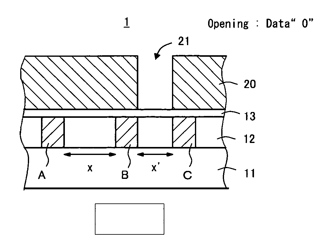
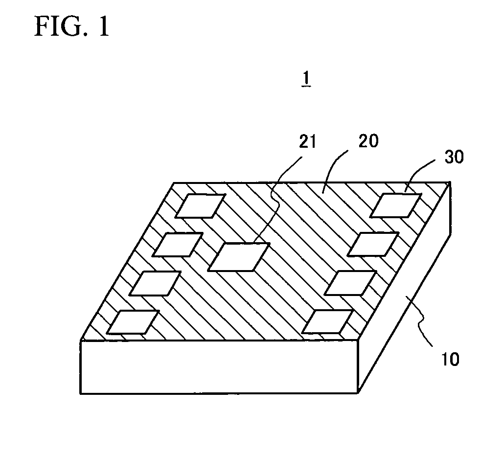
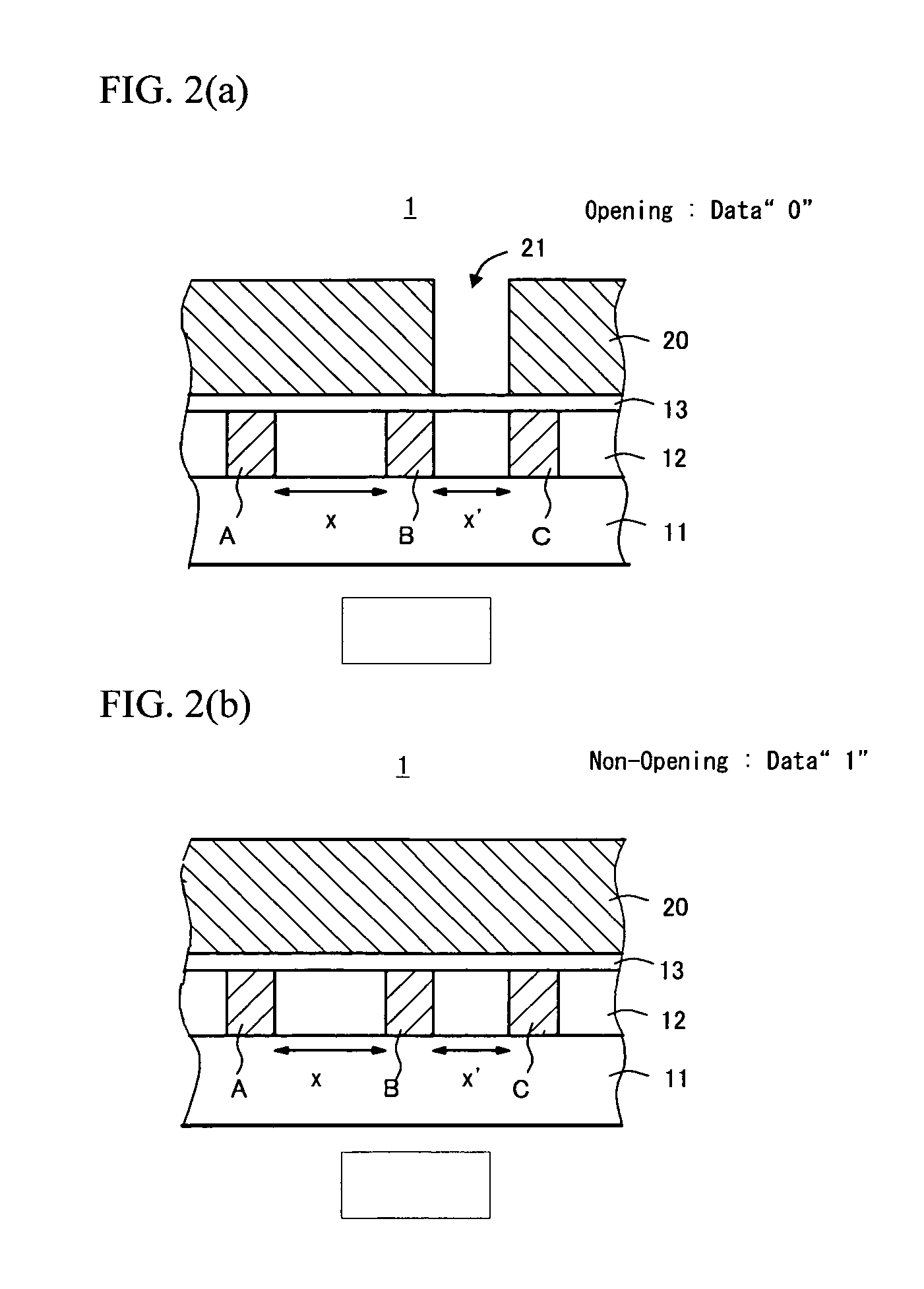
[0031]FIG. 1 is a view of a logic device (semiconductor die) subsequent to wafer processing thereof. The logic device 1 includes a semiconductor substrate 10 with a program layer 20 formed thereabove. An opening 21 is formed in the program layer 20 and pads 30 are formed on the program layer 20. A memory device of such a semiconductor device 1 includes a pair of metal interconnections and a dielectric film provided over the metal interconnections. The memory stores information to be determined by an electrostatic capacitance value that varies depending on whether there is an opening 21 in the program layer 20 provided above the pair of metal...


PUM


Abstract

A semiconductor device is provided which includes a pair of metal interconnections (B, C) provided above a semiconductor substrate (10), a program layer (20) provided over the pair of metal interconnections (B, C) and in which an opening (21) may be selectively formed in the program layer (20) on the basis of programming information, and a read circuit (40) reading the programming information by determining whether such an opening (21) is formed in the program layer (20) by utilizing an electrostatic capacitance between the pair of metal interconnections (B, C). The program layer (20) may be made of a material having a dielectric constant higher than that of air or the program layer (20) may be made of a conductor or a material having a dielectric constant lower than that of air. Thus, trimming information or information on a device identification (ID) can be stored, even if the semiconductor device is a logic device that does not have a memory transistor, by detecting the information that is determined by the electrostatic capacitance that varies depending on whether or not there is provided an opening (21).

Description

CROSS-REFERENCES TO RELATED APPLICATIONS[0001]This is a continuation of International Application No. PCT / JP2005 / 008058, filed Apr. 27, 2005 which was not published in English under PCT Article 21 (2).BACKGROUND OF THE INVENTION[0002]1. Field of the Invention[0003]This invention relates generally to semiconductor devices and data reading methods therefor, and fabricating methods of such semiconductor devices.[0004]2. Description of the Related Art[0005]Some conventional non-volatile memories have Contents Addressable Memory (CAM) cells that store device information such as device IDs used for various tests or device identification, or trimming data for adjusting the circuit characteristics with ease (such as disclosed in Japanese Patent Application Publication No. 2004-213872).[0006]A CAM cell is composed of a floating gate and a control gate stacked above a semiconductor substrate to form a gate with a source and a drain respectively formed in the semiconductor substrate at both si...

Claims


Application Information

Patent Timeline
Patent Type & Authority Patents(United States)
IPC IPC(8): H01L29/72
CPCH01L27/101
Inventor KASA, YASUSHI
Owner MONTEREY RES LLC
Why Eureka
Try Eureka