N channel JFET based digital logic gate structure

a gate structure and channel technology, applied in logic circuits, logic circuits characterised by logic functions, pulse techniques, etc., can solve problems such as parameter distribution issues precluded conventional direct coupling, current processing needs exceeding sic integrated circuit production capabilities, and inability to allow for high-integrated circuits

Active Publication Date: 2010-03-30
NASA THE UNITED STATES OF AMERICA AS REPRESENTEDTHE THE ADMINISTATOR OF
View PDF20 Cites 9 Cited by
  • Summary
  • Abstract
  • Description
  • Claims
  • Application Information

AI Technical Summary

Benefits of technology

[0010]An embodiment of the present invention is directed to an apparatus configured to create digital logic gates. The apparatus comprises a first field effect transistor, at a front end, whose source is tied to zero volts and whose drain is tied to voltage (Vdd) through a first resistor. The apparatus also comprises a second field effect transistor, following the front end, configured as a unity gain buffer whose drain is tied to the Vdd, whose gate is tied to a node connecting the first field effect transistor to the first resistor, and whose drain is tied to a series combination of a second resistor and a third resistor. For a logic false input, the output is at logic true and for a logic true input, the output is at logic false.
[0011]Another embodiment of the invention is directed to a method including placing, at a front end of an inverter, a first field effect transistor whose source is tied to zero volts and whose drain is tied to voltage (Vdd) through a first resistor. The method also includes placing, following the front end, a second field effect transistor configured as a unity gain buffer whose drain is tied to the Vdd, whose gate is tied to a node connecting the first field effect transistor to the first resistor, and whose drain is tied to a series combination of a second resistor and a third resistor. For a logic false input, the output is at logic true and for a logic true input, the output is at logic false.
[0012]Another embodiment of the invention is directed to an apparatus including placing means for placing, at a front end of an inverter, a first field effect transistor whose source is tied to zero volts and whose drain is tied to voltage (Vdd) through a first resistor. The apparatus also includes placing means for placing, following the front end, a second field effect transistor configured as a unity gain buffer whose drain is tied to the Vdd, whose gate is tied to a node connecting the first field effect transistor to the first resistor, and whose drain is tied to a series combination of a second resistor and a third resistor. For a logic false input, the output is at logic true and for a logic true input, the output is at logic false.

Problems solved by technology

Current processing needs exceed SiC integrated circuit production capabilities, which do not allow for highly integrated circuits.
These parameter distribution issues precluded conventional direct coupled and buffered direct coupled FET logic techniques which depend upon precise manipulation and matching of transistor channel widths.
The lack of precise device to device control over device parameters in discrete SiC JFET production and the lack of complementary devices created the need to use resistors as loads and as level shifters.

Method used


Image

  • N channel JFET based digital logic gate structure
  • N channel JFET based digital logic gate structure
  • N channel JFET based digital logic gate structure

Examples


Embodiment Construction

[0022]Reference will now be made to the embodiments of the present invention, examples of which are illustrated in the accompanying drawings.

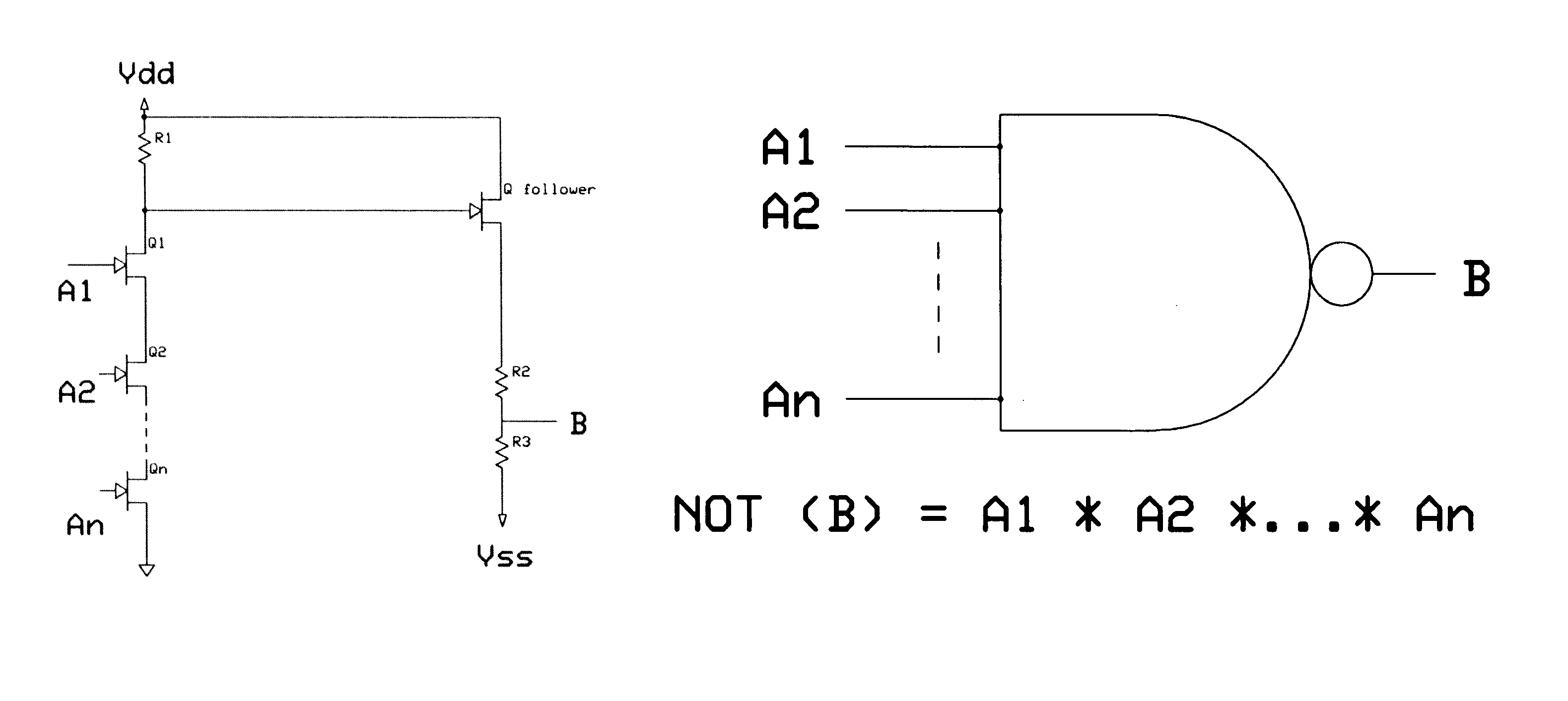
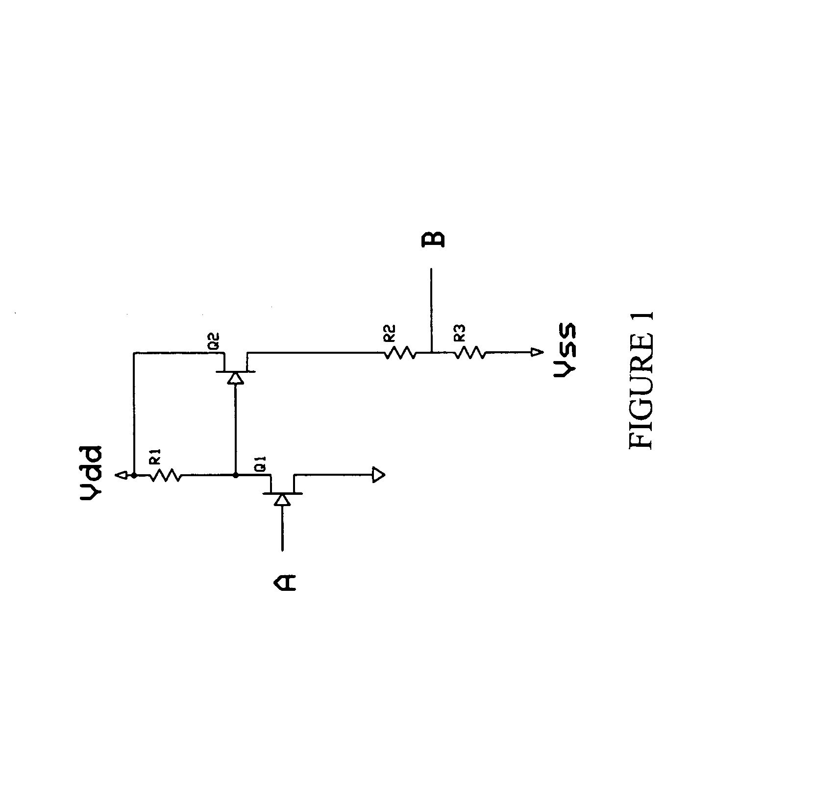
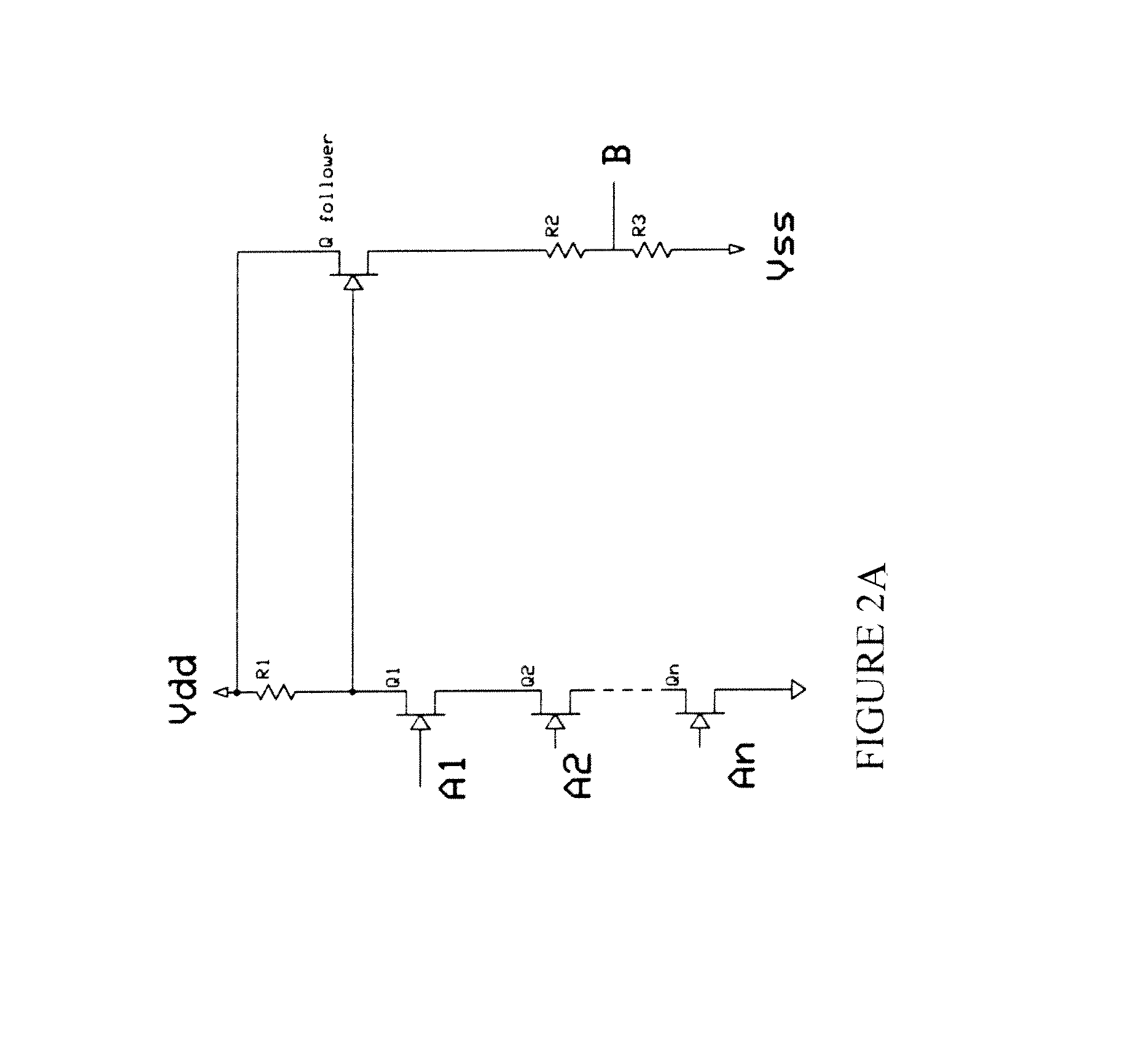
[0023]An embodiment of the present invention is directed to a circuit topography which is used to create digital logic gates using N (negatively doped) channel Junction Field Effect Transistors (JFETs) and load resistors, level shifting resistors and supply rails whose values are based on the direct current (DC) parametric distributions of those JFETs. This method has direct application to the current state of the art in high temperature, for example higher than 300° C., silicon carbide (SiC) device production. The ability to produce inverting and combinatorial logic enables the production of pulse and edge triggered latches. This scale of logic synthesis brings digital logic and state machine capabilities to devices operating in extremely hot environments like the surface of Venus, near hydrothermal vents, within nuclear reactors and within in...


PUM


Abstract

A circuit topography is presented which is used to create usable digital logic gates using N (negatively doped) channel Junction Field Effect Transistors (JFETs) and load resistors, level shifting resistors, and supply rails whose values are based on the direct current (DC) parametric distributions of those JFETs. This method has direct application to the current state of the art in high temperature, for example 300° C. to 500° C. and higher, silicon carbide (SiC) device production. The ability to produce inverting and combinatorial logic enables the production of pulse and edge triggered latches. This scale of logic synthesis would bring digital logic and state machine capabilities to devices operating in extremely hot environments, such as the surface of Venus, near hydrothermal vents, within nuclear reactors (SiC is inherently radiation hardened), and within internal combustion engines. The basic logic gate can be configured as a driver for oscillator circuits allowing for time bases and simple digitizers for resistive or reactive sensors. The basic structure of this innovation, the inverter, can be reconfigured into various analog circuit topographies through the use of feedback structures.

Description

STATEMENT OF GOVERNMENT INTEREST[0001]The invention described herein was made by an employee of the United States Government and may be manufactured and used by or for the Government of the United States of America for governmental purposes without the payment of any royalties thereon or therefor.BACKGROUND OF THE INVENTION[0002]1. Field of the Invention[0003]The present invention relates to a circuit topography which is used to create usable digital logic gates using N (negatively doped) channel Junction Field Effect Transistors (JFETs) and load resistors, level shifting resistors, and supply rails whose values are based on the direct current parametric distributions of those JFETs. This method has direct application to the current state of the art in high temperature (300° C. to 500° C. and higher) silicon carbide (SiC) device production.[0004]2. Description of the Related Art[0005]There are current reasons for placing intelligent processing near or within sources of high temperat...

Claims


Application Information

Patent Timeline
Patent Type & Authority Patents(United States)
IPC IPC(8): H03K19/20H03K19/094
CPCH03K19/094H03K19/20
Inventor KRASOWSKI, MICHAEL J.
Owner NASA THE UNITED STATES OF AMERICA AS REPRESENTEDTHE THE ADMINISTATOR OF
Why Eureka
Try Eureka