Automated design process and method for multi-rail cells and connections

Active Publication Date: 2010-04-06
SYNOPSYS INC +1
View PDF11 Cites 10 Cited by
  • Summary
  • Abstract
  • Description
  • Claims
  • Application Information

AI Technical Summary

Benefits of technology

[0008]Automated design process comprises steps of creating RTL source file including set of syntactic elements for voltage island connections of multi-rail cells, processing RTL source file according to effect of voltage island connections of multi-rail cells, and g

Problems solved by technology

Such inability to represent such an architectural choice of voltage elements in RTL inhibits development of design automation methods.
Hence, it is not possible to simulate, synthesize, perform physical design or formally verify semiconductor chip design implemented with multi-rail cells without hardship and risk of failure.
Voltages are often key functionality factors; and treating them as “non-functional” is thus problematic.

Method used


Image

  • Automated design process and method for multi-rail cells and connections
  • Automated design process and method for multi-rail cells and connections
  • Automated design process and method for multi-rail cells and connections

Examples


Embodiment Construction

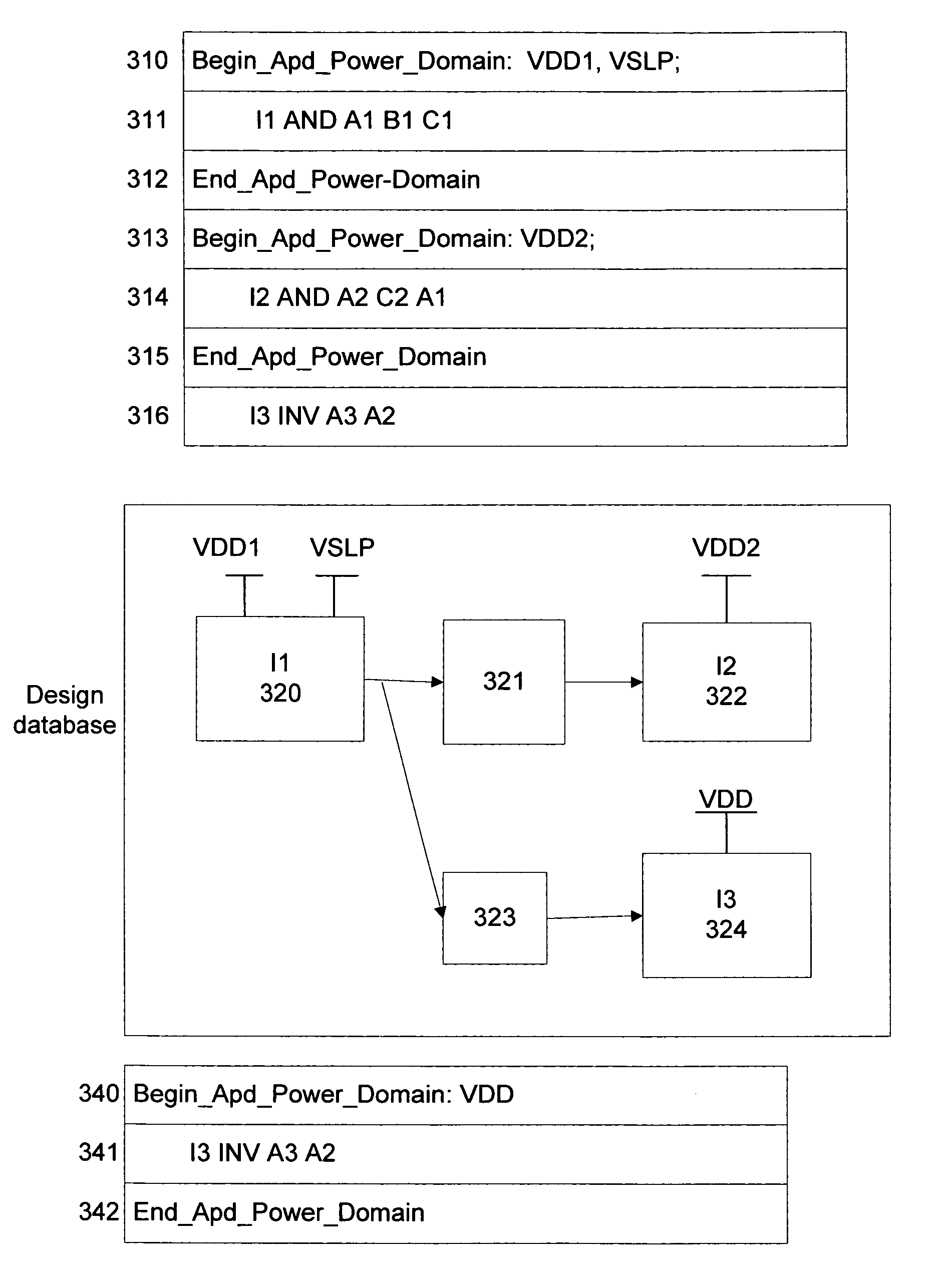
[0014]As used herein multi-rail cell is defined cell that has multiple voltage connections, other than power / ground connection. In CMOS there is driving voltage connection per transistor; driving voltage being defined as voltage that can charge / discharge output load of CMOS gate. Nevertheless cell may be coupled to other voltages connections such as retention, sleep, body bias, etc., which can alter circuit behavior and ability to charge / discharge output load. Such voltage connections do not often directly drive output of gate, i.e., provide current to charge / discharge output.

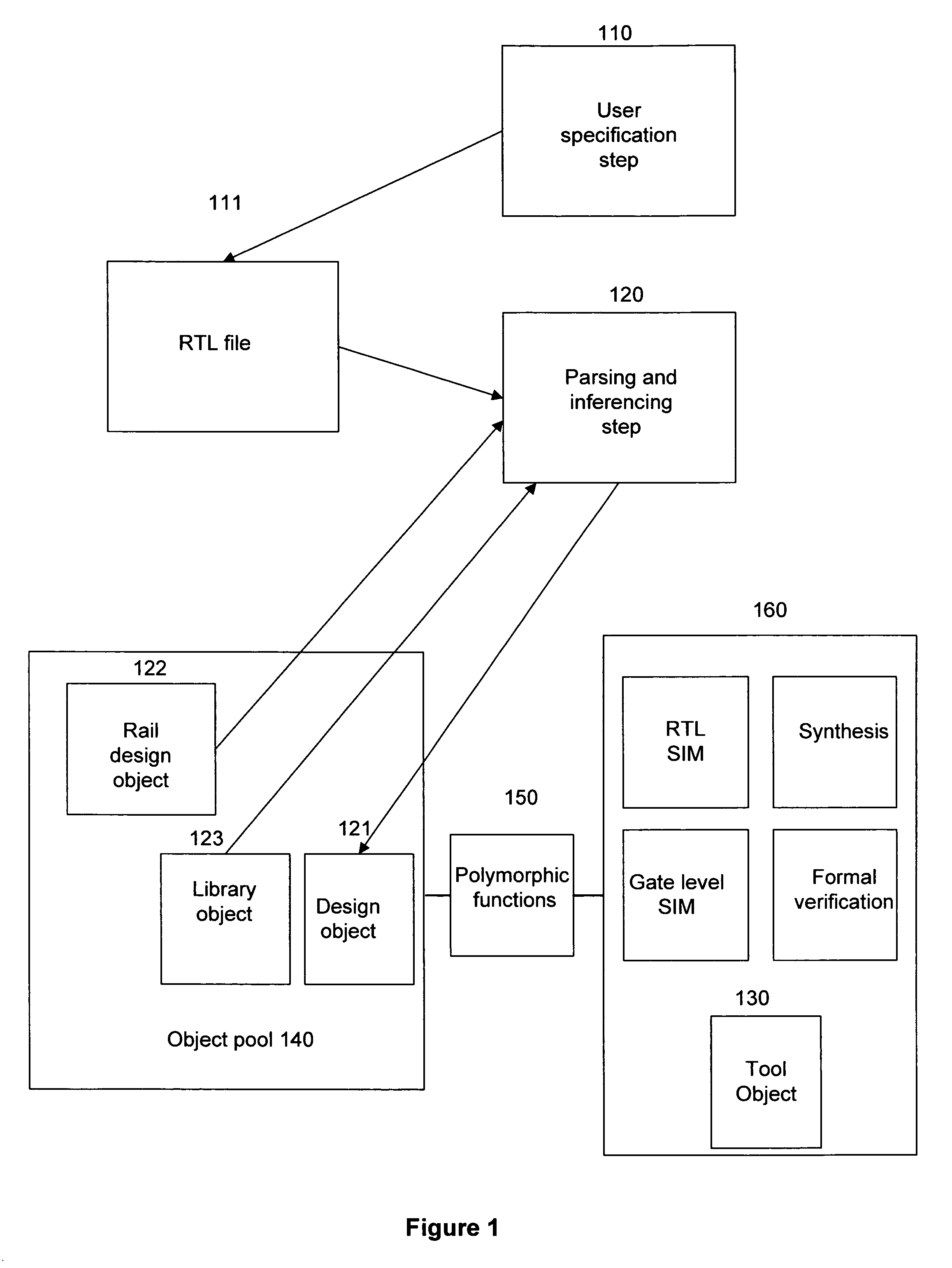
[0015]FIG. 1 operational process flow chart for automated design process comprises user specification step 110 that creates RTL file 111, parsing and / or inference step 120 that creates design object 121, and other implementation and / or verification steps 160. Parsing and inference step 120 creates design object 121 based on rail design object 122, library object 123, tool object 130 and / or object pool 140. Othe...


PUM


Abstract

Automated design process and method with set of syntactic elements compensates for inability to represent voltage island connection of multi-rail cells in RTL source files in traditional design process which inhibits development of design automation methods and causes hardship and risk of failure to simulate, synthesize, perform physical design or formally verify a semiconductor chip design implemented with multi-rail.

Description

BACKGROUND[0001]1. Field[0002]Invention relates to electronic design automation (EDA), particularly to automated design process and method for semiconductor chip implemented with multi-rail cells, wherein multi-rail circuit and logic design employ multi-VDD, back bias, sleep transistors, retention grids, etc.[0003]2. Related Art[0004]In semiconductor chip design, tools commonly classified as electronic design automation (EDA) software are used to provide means for automating design of Integrated Circuits (IC) and Systems on Chip (SoC). Tools are also used to provide means of automating task(s) of preparing design for manufacture on silicon.[0005]Moreover Hardware Description Languages (HDL) are used to model semiconductor chip and functions. Existing HDL technology places main function description of IC and SoC in Register Transfer Language (RTL) source files.[0006]RTL files do not include information about various “non-functional” aspects of the design. One of such “non-functional”...

Claims


Application Information

Patent Timeline
IPC IPC(8): G06F17/50
CPCG06F17/5045G06F30/30
Inventor JADCHERLA, SRIKANTHKOTNI, SRIRAM
Owner SYNOPSYS INC
Why Eureka
Try Eureka