Reducing stray capacitance in antenna element switching

a technology of antenna element and capacitance, applied in the field of wireless communications networks, can solve the problems of undesirable capacitance, stray capacitance, and the burden on wireless communications systems, and achieve the effect of reducing the stray capacitance of the pin diod

Inactive Publication Date: 2010-04-13
ARRIS ENTERPRISES LLC
View PDF221 Cites 40 Cited by
  • Summary
  • Abstract
  • Description
  • Claims
  • Application Information

AI Technical Summary

Benefits of technology

[0014]One exemplary embodiment is for an antenna array that includes an antenna element configured to receive an RF signal and a PIN diode coupled to the antenna element. Biasing the PIN diode influences the received RF signal. In the case of the PIN diode being forward biased, the received RF signal is cancelled at a stub coupled to the PIN diode by reflecting the RF signal out-of-phase within the stub. Cancellation of the RF signal may reduce stray capacitance of the PIN diode. An inductor may be further coupled to the stub thereby drawing the RF signal to the stub via the forward biased PIN diode.
[0016]Another exemplary embodiment is for a method for switching antenna elements within an array. An RF signal is received at an antenna element. A PIN diode coupled to the antenna element is thereby influencing the received RF signal. In the instance that the PIN diode is forward biased, the received RF signal may be cancelled at a stub coupled to the PIN diode. Cancellation may occur by reflecting the RF signal out-of-phase within the stub. By canceling the RF signal, stray capacitance of the PIN diode may be reduced.

Problems solved by technology

Wireless communications systems are burdened with an ever-increasing demand for higher data throughput.
The wireless link may be susceptible to interference from other access points and stations (nodes), other radio transmitting devices, changes or disturbances in the wireless link environment between the access point and the remote receiving node, and so forth.
In some instances, the interference may be of such significance as to force communications across the wireless link at a lower data rate or to completely disrupt the wireless link all together.
Stray capacitance is an undesirable capacitance existing between two conductors.
The occurrence and effects of stray capacitance are often overlooked during modeling and may lead to serious performance issues after a PCB and its constituent elements (e.g., radio equipment and antenna elements) are constructed and assembled.
Stray capacitance may result in greater noise, reduced frequency response, and even system instability.
The stray capacitance of PIN diodes in an antenna array, especially in a series of PIN diodes, may hinder the operation of the antenna array and / or the components thereon.
At a given operating frequency, a PIN diode with relatively low stray capacitance is typically more expensive than a PIN diode with higher stray capacitance.
In addition to expense, certain techniques for eliminating stray capacitance may require additional components to be located on or coupled to the PCB.
These additional components may increase difficulties related to manufacturing and design with respect to configuring various elements in a finite space.
These additional components, too, may increase the cost of manufacture.

Method used


Image

  • Reducing stray capacitance in antenna element switching
  • Reducing stray capacitance in antenna element switching
  • Reducing stray capacitance in antenna element switching

Examples


Embodiment Construction

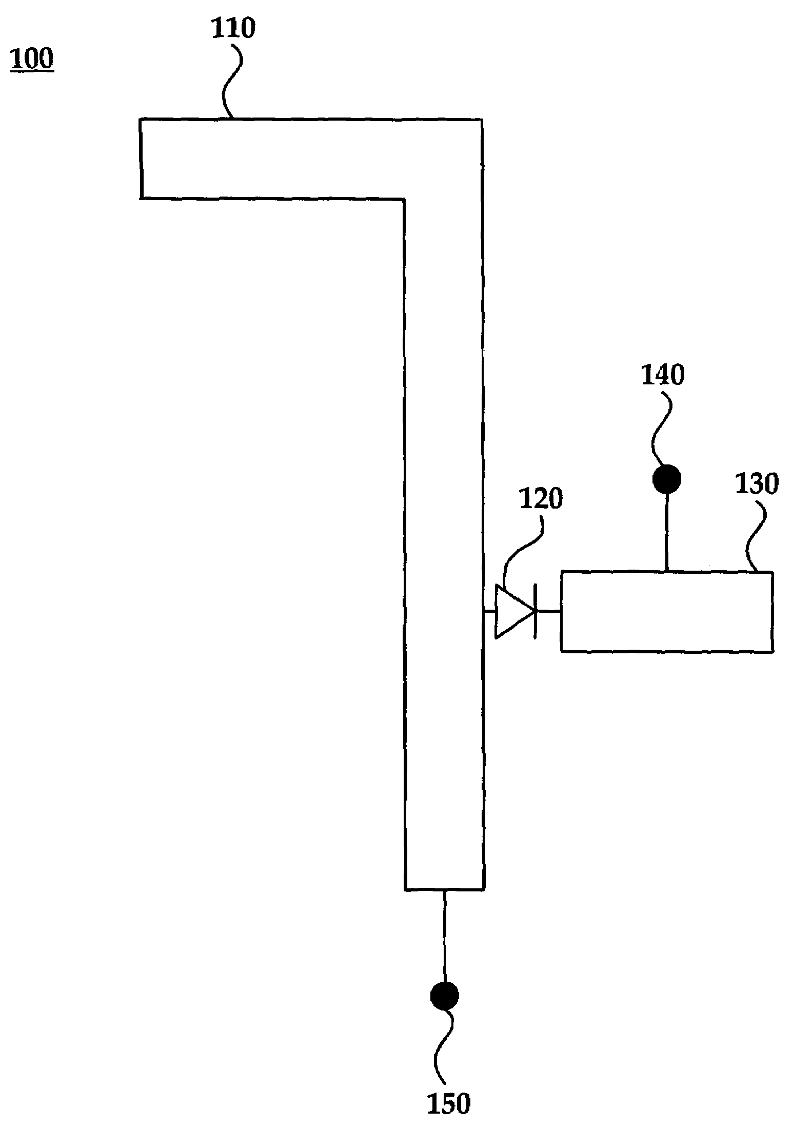
[0021]The disclosed antenna elements and antenna arrays utilizing such elements may be configured to receive an RF signal. A biased semiconductor device such as a PIN diode may be coupled to the antenna element receiving the RF signal. When forward biased or “on,” the PIN diode may behave as a variable resistor. Alternatively, the PIN diode may behave as a parallel plate capacitor when the diode is zero or reverse biased (“off”).

[0022]Subject to the bias of the aforementioned PIN diode, the RF signal may be reflected (e.g., via a forward bias) out-of-phase within a stub to cancel or reduce the received RF signal. By canceling or reducing the RF signal, the signal may no longer propagate through the antenna element thereby functionally turning the element “off.”

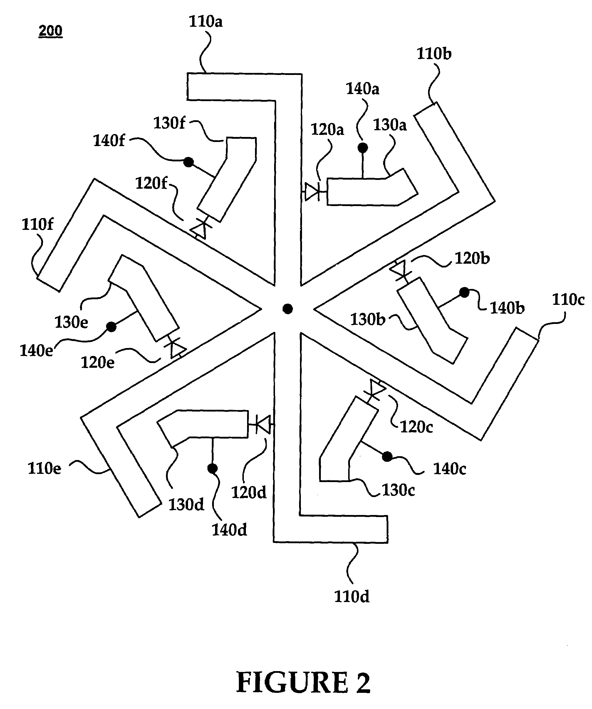
[0023]PIN diodes may be used in series to function as “RF switches” for an antenna with multiple antenna elements. An antenna array may include any number of antenna elements that are controlled individually, collectively, or ...


PUM


Abstract

An antenna array may include an antenna element configured to receive an RF signal. A PIN diode may selectively couple the antenna element to an RF source. Biasing the PIN diode may cancel the received RF signal at a stub coupled to the diode thereby reducing stray capacitance of the PIN diode. A method for switching antenna elements is also disclosed. A PIN diode coupled to an antenna element is biased thereby reflecting the received RF signal out-of-phase within a stub such that the signal is canceling and stray capacitance of the PIN diode is reduced.

Description

CROSS-REFERENCE TO RELATED APPLICATIONS[0001]The present application claims the priority benefit of U.S. provisional patent application No. 60 / 795,919 filed Apr. 28, 2006 and entitled “Systems and Methods for Switching Antenna Elements.”[0002]The present application is also a continuation-in-part and claims the priority benefit of U.S. patent application Ser. No. 11 / 010,076 filed Dec. 9, 2004 now U.S. Pat. No. 7,292,198 and entitled “System and Method for an Omnidirectional Planar Antenna Apparatus with Selectable Elements” and is also a continuation-in-part and claims the priority benefit of U.S. patent application Ser. No. 11 / 041,145 filed Jan. 21, 2005 now U.S. Pat. No. 7,362,280 and entitled “System and Method for a Minimized Antenna Apparatus with Selectable Elements.” U.S. patent application Ser. No. 11 / 010,076 and 11 / 041,145 both claim the priority benefit of U.S. provisional patent application No. 60 / 602,711 filed Aug. 18, 2004 and entitled “Planar Antenna Apparatus for Isot...

Claims


Application Information

Patent Timeline
Patent Type & Authority Patents(United States)
IPC IPC(8): H01Q21/00
CPCH03H7/383H01P1/15
Inventor SHTROM, VICTOR
Owner ARRIS ENTERPRISES LLC
Why Eureka
Try Eureka