Semiconductor device and method for manufacturing same

a semiconductor and semiconductor technology, applied in the direction of semiconductor devices, electrical devices, transistors, etc., can solve the problems of uniform etching, unsatisfactory transistor properties, and unsatisfactory etching of semiconductor layers in both ends corresponding to end resists b>15/b>, etc., to achieve excellent operation properties, high reliability, and improve the flatness of gate electrodes

Active Publication Date: 2010-04-20
GK BRIDGE 1
View PDF11 Cites 44 Cited by
  • Summary
  • Abstract
  • Description
  • Claims
  • Application Information

AI Technical Summary

Benefits of technology

[0013]Furthermore, in a conventional process for manufacturing a fin-type MISFET, semiconductor layers in both ends may become narrower during etching. FIG. 6(a) shows a state where after forming a resist pattern, a semiconductor layer is formed by etching. FIG. 6(b) is a cross-sectional view taken on line A-A′ of FIG. 6(a). FIG. 6(c) shows a state where a semiconductor layer is formed in an MISFET having common source / drain regions by etching as described above. In FIG. 6, semiconductor layers 18 in both ends have a width (“a” in FIG. 6) smaller than a width in the other semiconductor layers (a′). It occurs due to asymmetric microloading effect.
[0043]In the present invention, the width of the source / drain regions in the semiconductor layers in the first semiconductor region can be increased to facilitate alignment of a contact and to provide a semiconductor device exhibiting excellent operation stability. Furthermore, a parasitic resistance can be reduced.

Problems solved by technology

However, in a conventional process for manufacturing a fin-type MISFET, when forming a plurality of semiconductor layers, semiconductor layers in both ends have forms and impurity concentrations different from those in the other semiconductor layers, sometimes leading to undesirable transistor properties.
For example, when a semiconductor layer is formed using a resist mask, etching may be ununiform.
Therefore, in a later etching step, the semiconductor layers in both ends corresponding to these end resists 15 may not be uniformly etched.

Method used


Image

  • Semiconductor device and method for manufacturing same
  • Semiconductor device and method for manufacturing same
  • Semiconductor device and method for manufacturing same

Examples


Embodiment Construction

Semiconductor Device

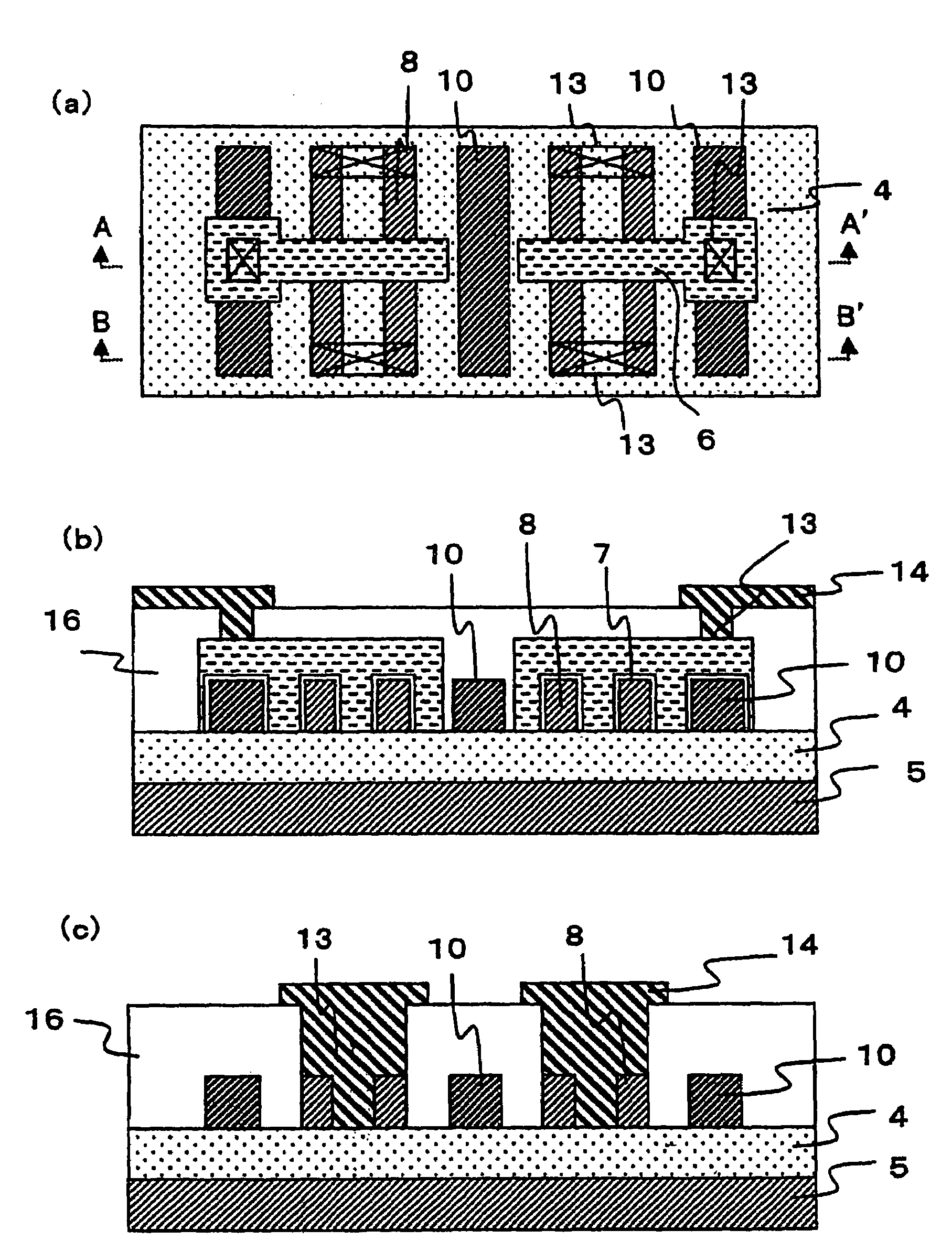
[0075]In a semiconductor device of the present invention, it has a first semiconductor region and second semiconductor region in both sides of the first semiconductor region in a direction perpendicular to a channel current direction and a channel region is formed at least a side surface of a semiconductor layer in the first semiconductor region.

[0076]FIG. 9 shows an example of a semiconductor device according to the present invention. FIG. 9(a) is a plan view of a semiconductor device having a plurality of semiconductor layers 8 as the first semiconductor region. FIG. 9(b) is a cross-sectional view taken on line A-A′ of FIG. 9(a); FIG. 9(c) is a cross-sectional view taken on line B-B′ of FIG. 9(a); and FIG. 9(d) is a cross-sectional view taken on line C-C′ of FIG. 9(a) (FIG. 9(a) does not show an interlayer insulating film 16 or an interconnection 14. In addition, FIGS. 9(a) to (c) do not show a gate sidewall 44).

[0077]This semiconductor device is formed using a...


PUM


Abstract

A semiconductor device comprising a first semiconductor region and a second semiconductor region,(a) wherein a field effect transistor is comprised of the first semiconductor region comprising at least one semiconductor layer(s) protruding upward from a substrate, a gate electrode(s) formed via an insulating film such that the gate electrode(s) strides over the semiconductor layer(s) and source / drain regions provided in the semiconductor layer(s) on both sides of the gate electrode(s), whereby a channel region is formed in at least both sides of the semiconductor layer(s),(b) wherein the second semiconductor region comprises semiconductor layers protruding upward from the substrate and placed, at least opposing the first semiconductor region at both ends in the direction perpendicular to a channel current direction and the side surface of the semiconductor layers facing the first semiconductor region is parallel to the channel current direction.

Description

TECHNICAL FIELD[0001]The present invention relates to a semiconductor device having a field effect transistor with excellent operation properties and reliability, as well as a manufacturing process thereof.BACKGROUND OF THE INVENTION[0002]There has been developed a fin-type MIS type field effect transistor (hereinafter, referred to as “MISFET”) having a protrusion consisting of a semiconductor layer in which a main channel region is formed in side surface of the protrusion. A fin-type MISFET is known to be advantageous in terms of size reduction as well as improvement in various properties such as improvement in cutoff properties or carrier mobility and reduction in short channel effect and punch-through.[0003]FIG. 1 shows a semiconductor device containing an MISFET having a single structure comprising a single cuboid semiconductor layer. FIG. 1(a) is a plan view of this semiconductor device and FIG. 1(b) is a cross-sectional view taken on line A-A′ of FIG. 1(a). In the structure sh...

Claims


Application Information

Patent Timeline
Patent Type & Authority Patents(United States)
IPC IPC(8): H01L27/088H01L21/336H01L29/786
CPCH01L29/41791H01L29/785H01L29/66795H01L2029/7858H01L29/6681
Inventor YAMAGAMI, SHIGEHARUWAKABAYASHI, HITOSHITAKEUCHI, KIYOSHIOGURA, ATSUSHITANAKA, MASAYASUNOMURA, MASAHIROTAKEDA, KOICHITATSUMI, TORUWATANABE, KOJITERASHIMA, KOICHI
Owner GK BRIDGE 1
Why Eureka
Try Eureka