
CdZnTe device using constrained design for high-flux x-ray spectroscopic imaging applications

a cdznte and x-ray technology, applied in the direction of radiation controlled devices, instruments, optical radiation measurement, etc., can solve the problems of reversible count paralysis failure, high count rate of photon flux fields within the cdznte detector,

Active Publication Date: 2010-04-27
PRODUCE
View PDF1 Cites 10 Cited by
  • Summary
  • Abstract
  • Description
  • Claims
  • Application Information

AI Technical Summary

Benefits of technology

The design enables CdZnTe detectors to handle photon fluxes exceeding 20 million counts / s / mm2 without polarization, significantly enhancing their performance in high-flux imaging applications by effectively managing charge transport and electric fields.

Problems solved by technology

However, imaging applications typically require photon flux fields that generate very high count rates within the CdZnTe detector.
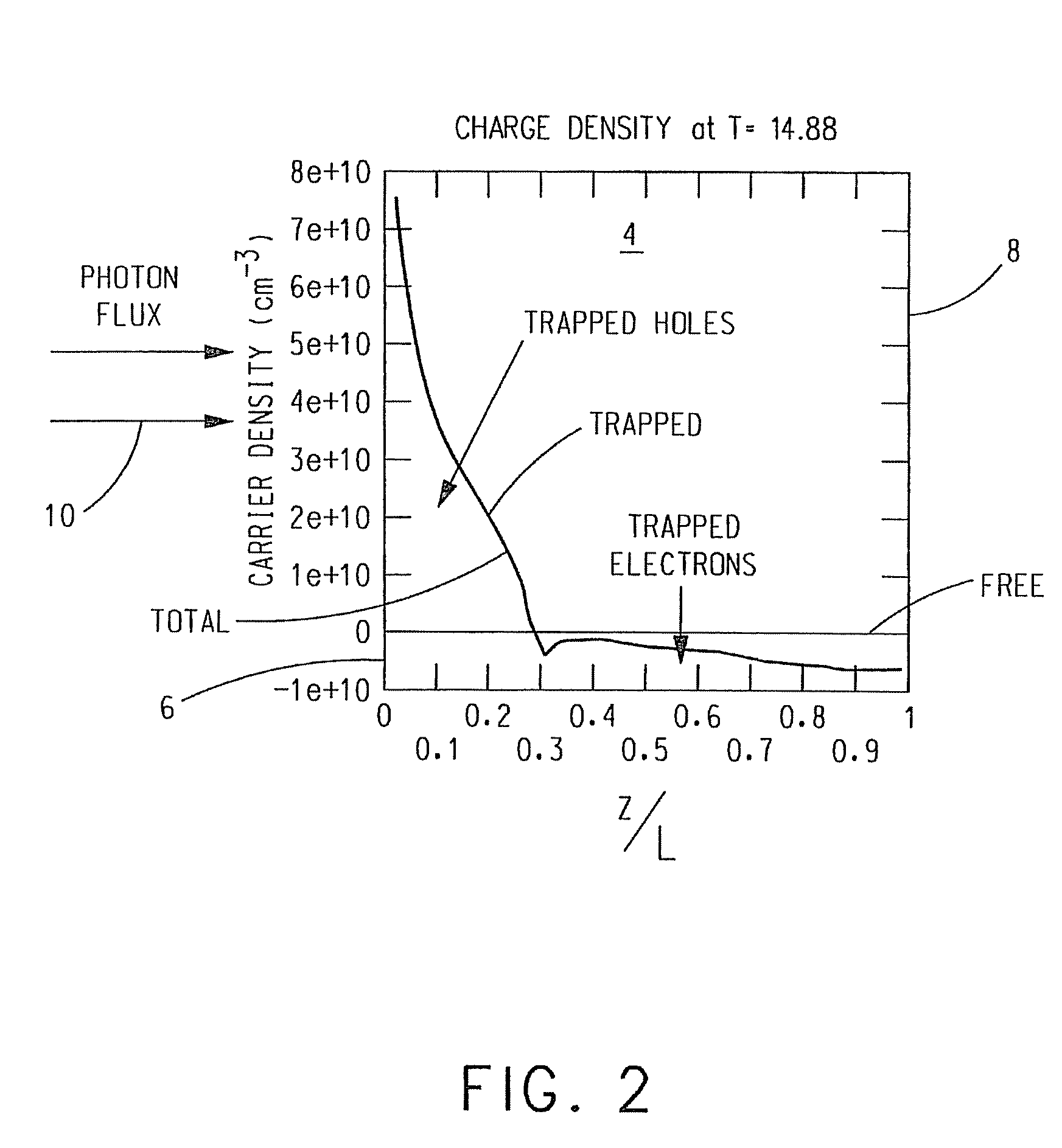
One of the challenges in applying pulse mode CdZnTe detectors to applications requiring such high count rates is avoiding a build up of “space charge” within the CdZnTe crystal structure that collapses the electric field and results in a reversible count paralyzation failure (i.e., polarization).

Method used


Image

  • CdZnTe device using constrained design for high-flux x-ray spectroscopic imaging applications
  • CdZnTe device using constrained design for high-flux x-ray spectroscopic imaging applications
  • CdZnTe device using constrained design for high-flux x-ray spectroscopic imaging applications

Examples


Embodiment Construction

[0023]The present invention will be described with reference to the accompanying figures where like reference numbers correspond to like elements.

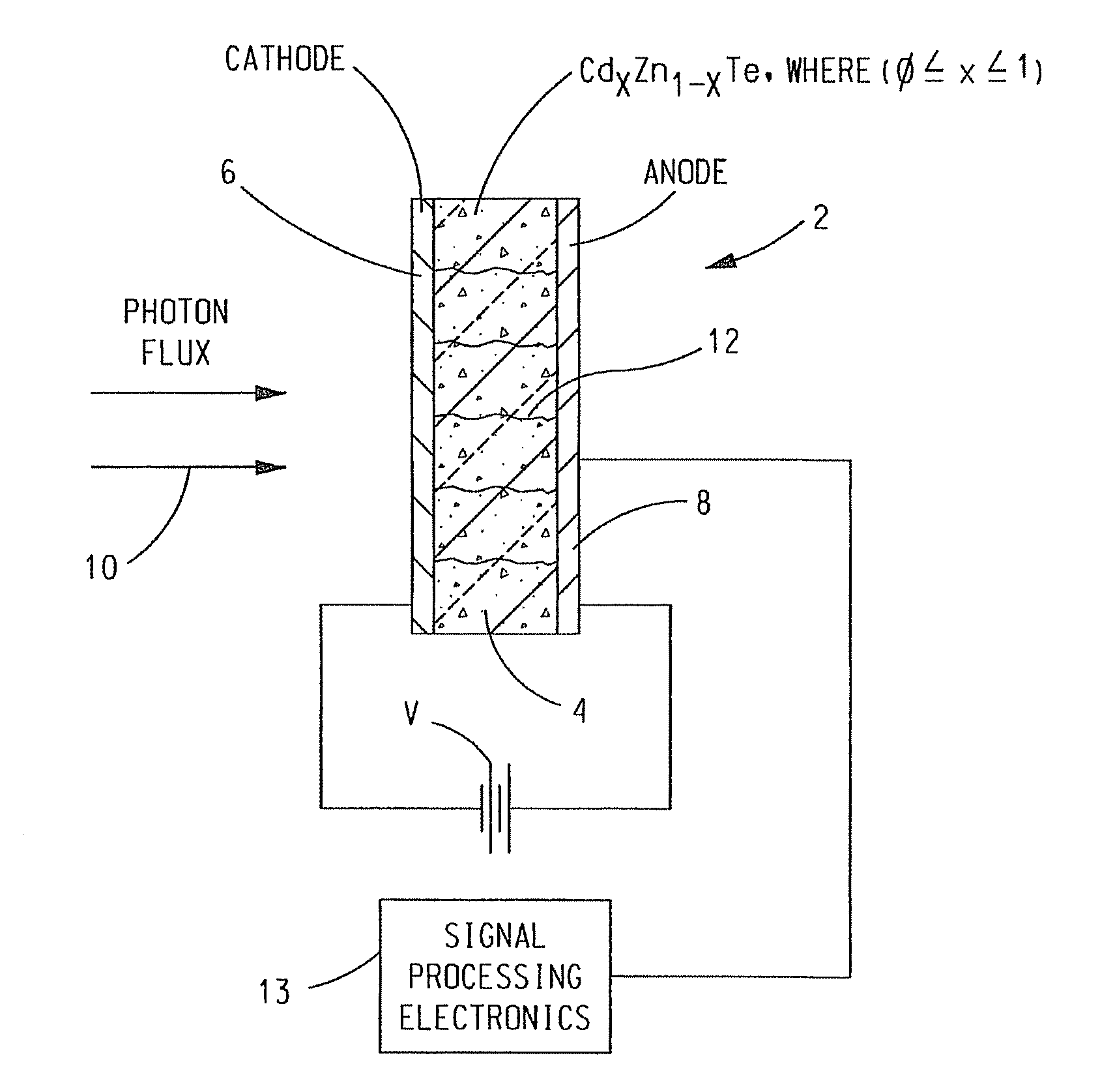
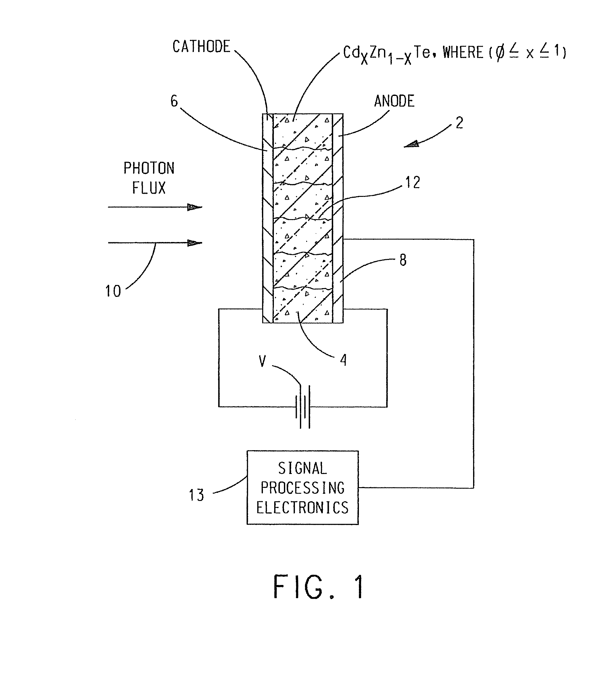
[0024]With reference to FIG. 1, a CdZnTe single crystal detector 2 includes a core material 4 of Cd1-xZnxTe, where (0≦x6 and a conducting anode terminal 8. Cathode 6 can be continuous or pixilated. Similarly, anode 8 can be continuous or pixilated. Cathode 6 and anode 8 are biased by a DC voltage V in a manner known in the art whereupon an electric field 12 is produced between cathode 6 and anode 8 in core material 4. In response to interaction between core material 4 and photon flux 10 (e.g., without limitation, x-ray radiation) entering core material 4 via cathode 6, electron-hole pairs are generated in core material 4. Electric field 12 attracts electrons generated in core material 4 to anode 8 for detection and processing by suitable signal processing electronics 13, which converts the electrons attracted to anode 8 into a number of co...


PUM


Abstract

A CdZnTe photon counting detector includes a core material of Cd1-xZnxTe, where (0≦x<1), an anode terminal on one side of the core material and a cathode terminal on a side of the core material opposite the anode terminal. At least one of the following is selected in the design of the detector as a function of the maximum sustainable photon flux the core material is able to absorb in operation while avoiding polarization of the core material: electron lifetime-mobility product of the core material; de-trapping time of the core material; a value of a DC bias voltage applied between the anode and the cathode; a temperature of the core material in operation; a mean photon flux density to be absorbed by the core material in operation; and a thickness of the core material between the anode and the cathode.

Description

CROSS REFERENCE TO RELATED APPLICATION[0001]This application claims benefit of U.S. Provisional Application No. 60 / 967,668, entitled “CdZnTe Device Using Constrained Design For High-Flux X-Ray Spectroscopic Imaging Applications”, filed Sep. 6, 2007, which is hereby incorporated by reference in its entirety.GOVERNMENT LICENSE RIGHTS[0002]The U.S. Government has a paid-up license in this invention and the right in limited circumstances to require the patent owner to license others on reasonable terms as provided for by the terms of contract DAAE 30 03 C 1171 awarded by U.S. Army Armament Research, Development, and Engineering Center (ARDEC).BACKGROUND OF THE INVENTION[0003]There is a growing interest in the potential of pulse mode CdZnTe crystalline detectors for high-flux high-speed energy selective or hyper-spectral x-ray imaging. The energy sensitivity provided by the Cd1-xZnxTe, where (0≦x<1), material forming these detectors opens up a range of new potential applications for t...

Claims


Application Information

Patent Timeline
Patent Type & Authority Patents(United States)
IPC IPC(8): H01L27/146G01J5/20
CPCG01T1/24
Inventor BALE, DEREK S.SOLDNER, STEPHEN A.SZELES, CSABA
Owner PRODUCE
Learn More