Heterojunction bipolar transistor having (In)(Al) GaAsSb/InGaAs base-collector structure

a bipolar transistor and base-collector technology, applied in the direction of basic electric elements, electrical apparatus, semiconductor devices, etc., can solve the problems of difficult to achieve high current density, difficult to obtain high current density, and hinder electrons, so as to achieve effective infusing electrons, improve electron transference, and high drift velocity

Active Publication Date: 2010-04-27
WIN SEMICON
View PDF7 Cites 2 Cited by
  • Summary
  • Abstract
  • Description
  • Claims
  • Application Information

AI Technical Summary

Benefits of technology

[0006]The main purpose of the present invention is to effectively infusing electrons from a base structure into a collector structure while an electron transference is improved with a high drift velocity in a low electric-field collector area.
[0009]Fourth purpose of the present invention is to lower a discontinuous conduction band of a junction between a collector I of InP and a collector II of InGaAs in a composite collector structure for increasing a current density.

Problems solved by technology

When electrons pass through a base structure of a general single HBT, electrons are not quickly transferred to a collector structure; and, owing to the continuous valence band of both two HBTs, holes are hard to be stopped from spreading from the base into the collector under a high current infused, so that a high current density is hard to be obtained.
However, because of a discontinuous conduction band in a base-collector interface, electrons are still hindered to a certain extent during the transference for obtaining a better transferring speed, not to mention that a high current density are hard to be achieved either.
Hence, the prior arts do not fulfill all users' requests on actual use.

Method used


Image

  • Heterojunction bipolar transistor having (In)(Al) GaAsSb/InGaAs base-collector structure
  • Heterojunction bipolar transistor having (In)(Al) GaAsSb/InGaAs base-collector structure
  • Heterojunction bipolar transistor having (In)(Al) GaAsSb/InGaAs base-collector structure

Examples


Embodiment Construction

[0024]The following descriptions of the preferred embodiments are provided to understand the features and the structures of the present invention.

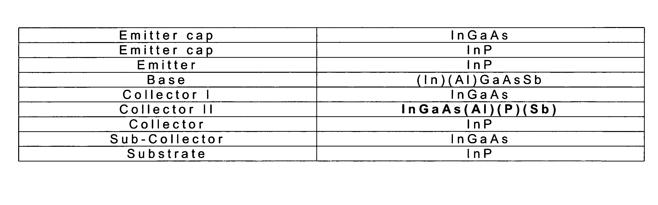
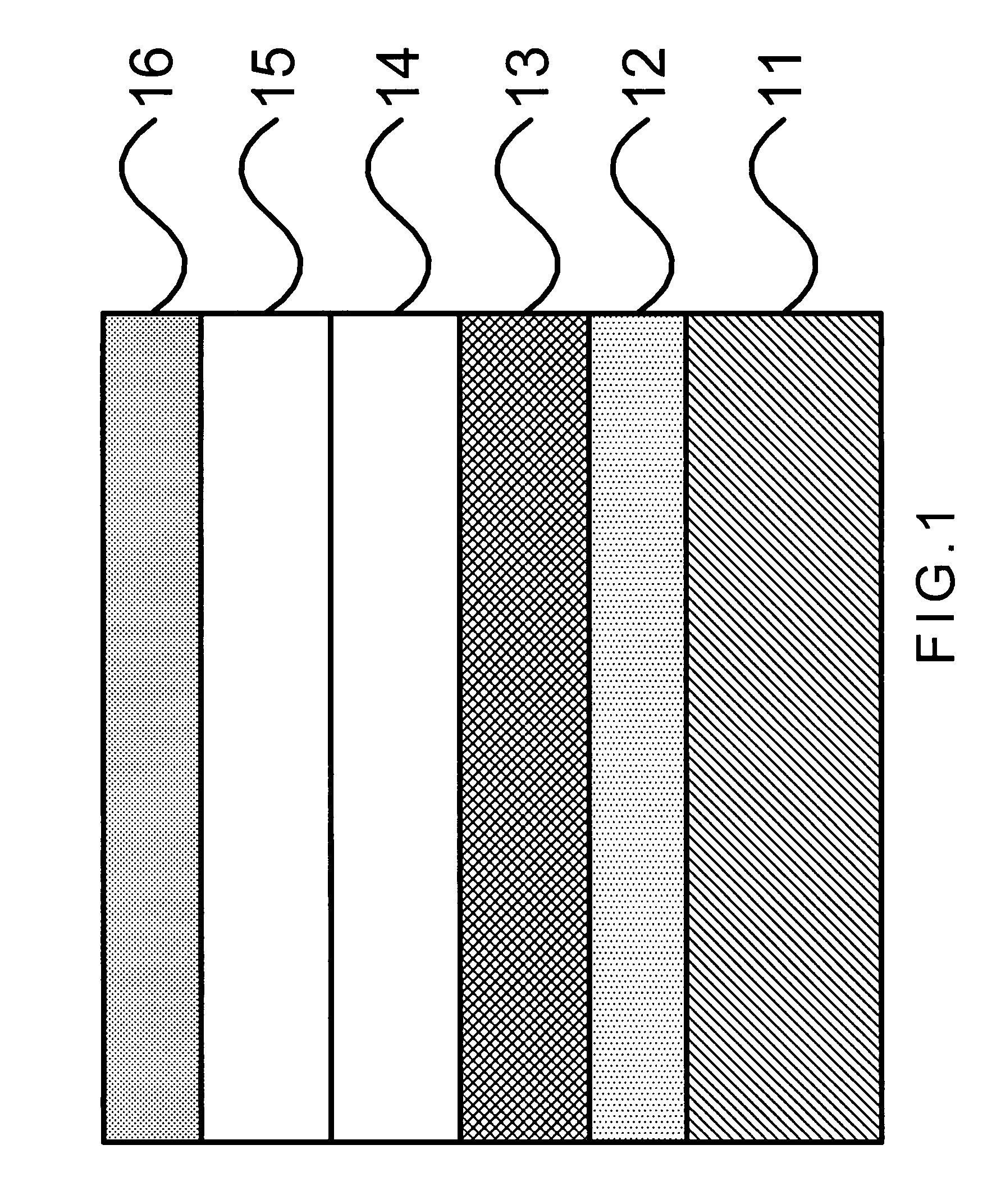
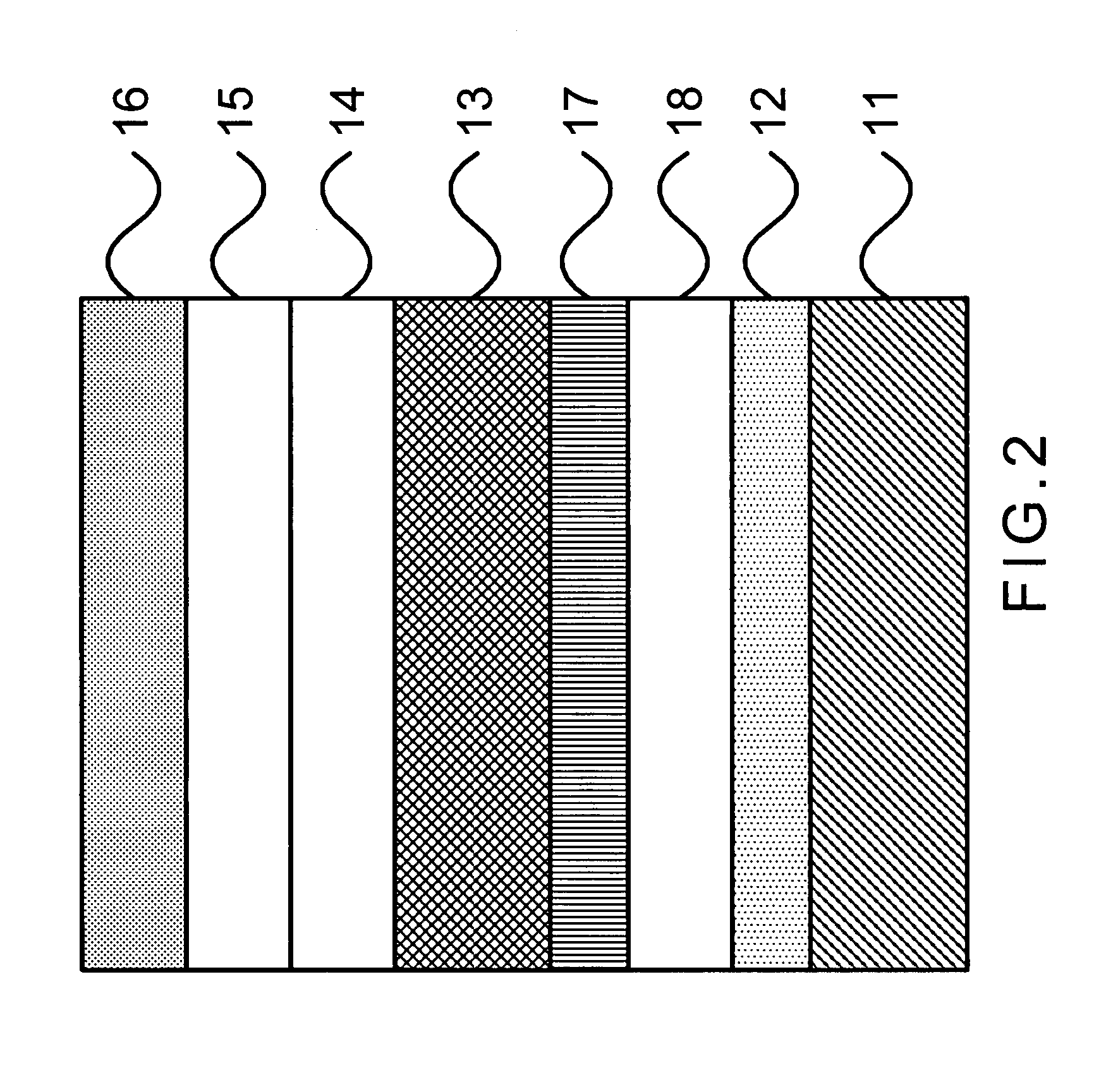
[0025]Please refer to FIG. 1 and FIG. 2, which are structural views showing a heterojunction bipolar transistor (HBT) having an (In)(Al)GaAsSb / InGaAs base-collector structure; and the HBT further comprising a second collector structure and a third collector structure according to the present invention. As shown in the figures, the present invention is an HBT having an (In)(Al)GaAsSb / InGaAs base-collector structure, comprising a substrate 11, a sub-collector contact layer 12, a first collector structure 13, a base structure 14, an emitter structure 15 and an emitter contact layer 16.

[0026]As shown in FIG. 2, a second collector structure 17 and a third collector structure 18 are added between the first collector structure 13 and the sub-collector contact layer 12.

[0027]The base structure 14 is grown on the first collector structure 13 throug...


PUM


Abstract

A heterojunction bipolar transistor (HBT) has a (In)(Al)GaAsSb / InGaAs base-collector structure. A discontinuous base-collector conduction band forms a built-in electric field to infuse electrons into a collector structure effectively, while a discontinuous base-collector valence band prevents holes from spreading into the collector structure at the same time. Thus, a current density is increased. In addition, the small offset voltage of the base-emitter and base-collector junctions reduce a power consumption.

Description

FIELD OF THE INVENTION[0001]The present invention relates to a heterojunction bipolar transistor (HBT); more particularly, relates to obtaining an HBT having a high cut-off frequency and a low power dissipation.DESCRIPTION OF THE RELATED ARTS[0002]Traditionally, an InGaAs single HBT is the transistor having the highest cut-off frequency, while its collector structure is usually used as a part of an optical electric integrated circuit.[0003]In FIG. 10 and FIG. 11, views of a general single HBT and a general collector-base graded single HBT are shown. When electrons pass through a base structure of a general single HBT, electrons are not quickly transferred to a collector structure; and, owing to the continuous valence band of both two HBTs, holes are hard to be stopped from spreading from the base into the collector under a high current infused, so that a high current density is hard to be obtained.[0004]FIG. 12 is a structural view of a general InGaAs composite collector bipolar tra...

Claims


Application Information

Patent Timeline
Patent Type & Authority Patents(United States)
IPC IPC(8): H01L31/0256
CPCH01L29/201H01L29/7371H01L29/205
Inventor WANG, SHENG-YUCHYI, JEN-INNCHENG, SHU-HAN
Owner WIN SEMICON
Why Eureka
Try Eureka