
Method and device for interconnect radio frequency power sic filed effect transistors

A field effect transistor, radio frequency power technology, applied in the fields of electric solid device, semiconductor device, semiconductor/solid state device manufacturing, etc., can solve problems such as harmful characteristics of transistors

Inactive Publication Date: 2002-07-17
INFINEON TECH AG
View PDF0 Cites 0 Cited by
  • Summary
  • Abstract
  • Description
  • Claims
  • Application Information

AI Technical Summary

Problems solved by technology

Especially parasitic source inductance is detrimental to transistor characteristics

Method used


Image

  • Method and device for interconnect radio frequency power sic filed effect transistors
  • Method and device for interconnect radio frequency power sic filed effect transistors
  • Method and device for interconnect radio frequency power sic filed effect transistors

Examples


Embodiment Construction

[0012] DETAILED DESCRIPTION OF THE PREFERRED EMBODIMENT

[0013] Active devices for high-frequency power amplification are widely used in the output section of communication systems. At high power levels, typically in excess of 1 kW, vacuum tube or other forms of amplification are employed. Traveling wave tubes (TWTs) or klystrons are used for power levels up to 10 MW. At relatively low power levels, solid-state transistors are used for almost all RF power amplification. High-frequency transistors were first fabricated in germanium in the late 1950s, but were quickly replaced by silicon bi-transistors in the early 1960s and have continued to dominate RF power, see the paper H.F. Cooke, "Microwave Transistors: Theory and Design", Proc. IEEE, vol.59, p.1163, Aug.1971.

[0014] For cellular radio communications, silicon bipolar transistors completely dominate base station output amplifiers and enable robust performance up to at least 2GHz with good stability, utilization, and ...


PUM


Abstract

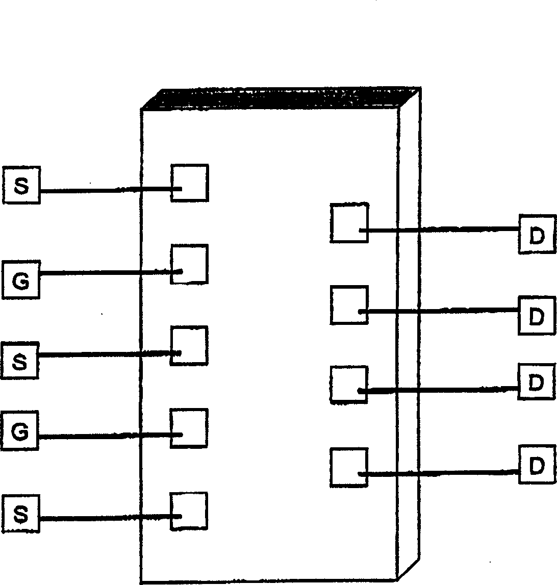
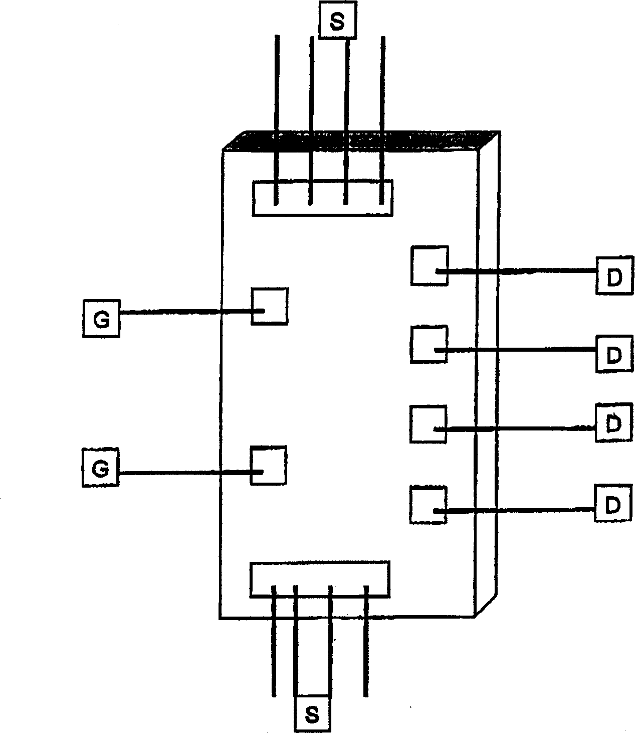
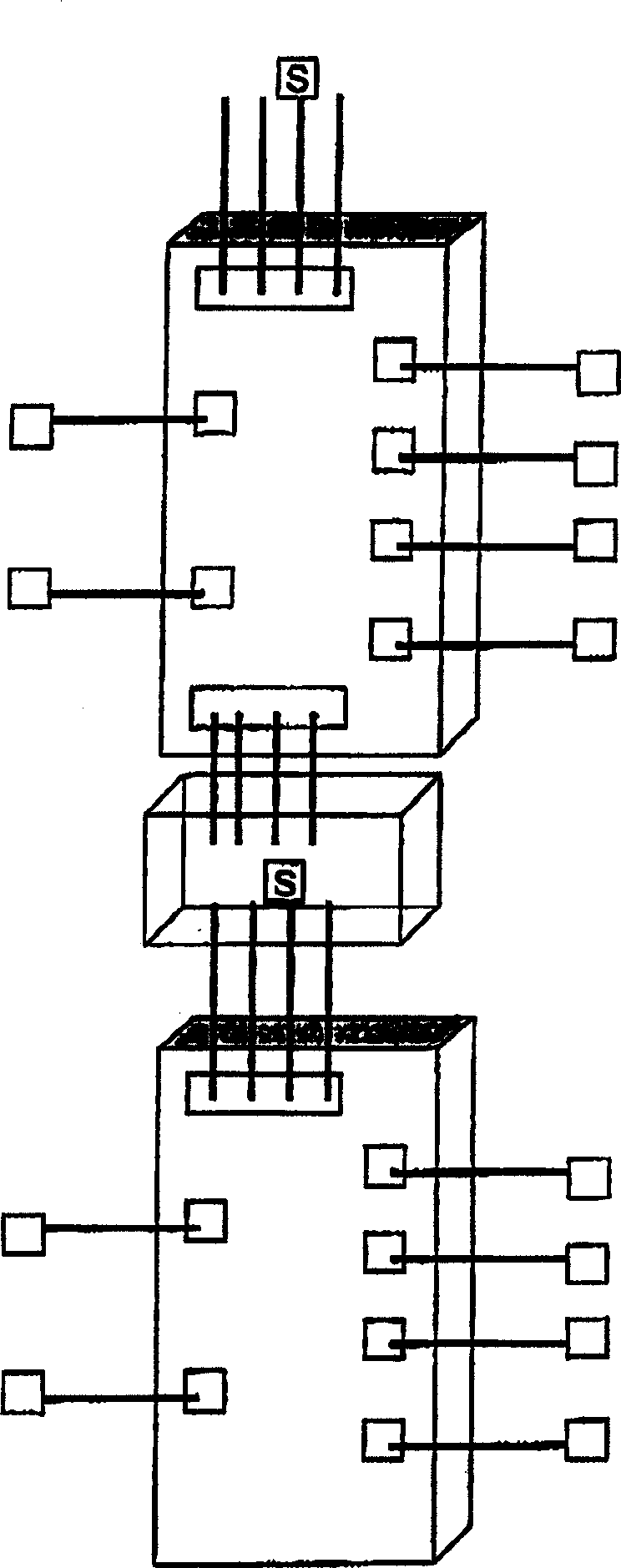
The present invention relates to a method and device for interconnecting radio frequency power SiC field effect transistors. To improve the parasitic source inductance advantage is taken of the small size of the transistors, wherein the bonding pads are placed on both sides of the die in such a way that most of the source bonding wires (6) go perpendicularly to the gate and drain bonding wires (7, 8). Multiple bonding wires can be connected to the source bonding pads, reducing the source inductance. An additional advantage comes from such arrangement by reducing the mutual inductance between source / gate and between source / drain due to the orthogonal wire placement.

Description

field of invention [0001] The invention relates to an interconnection method and device of a radio frequency power silicon carbide field effect transistor, the device includes an interconnection design of a radio frequency power silicon carbide field effect transistor and a radio frequency power silicon carbide field effect transistor with the interconnection design. background of the invention [0002] Silicon carbide (SiC) transistors have begun to replace Si and GaAs transistors for power generation at GHz frequencies. It has been foreseen and experimentally shown that silicon carbide transistors, relying on excellent material properties, are capable of handling much higher powers than the other types of transistors mentioned, i.e. transistors of the same size can produce several times higher power . To take full advantage of the advantages of the SiC die in the actual transistor package, the die-to-package connection should also be modified. Utilizing a conventional ME...

Claims


Application Information

Patent Timeline
IPC IPC(8): H01L23/15H01L23/64H01L23/66H01L25/07H01L25/18
CPCH01L2924/01015H01L2924/01032H01L2223/6644H01L2924/01023H01L2224/0603H01L2924/01082H01L2924/30105H01L24/06H01L2224/05553H01L2224/0401H01L2924/19041H01L2924/30107Y10S438/977H01L24/49H01L2924/10272H01L2924/19043H01L2924/3011H01L2224/48137H01L24/48H01L2924/01079H01L2223/6611H01L2224/48011H01L2924/01033H01L2924/01006H01L23/66H01L2924/10329H01L2924/01074H01L2924/01078H01L2224/49111H01L2924/01014H01L2224/49175H01L23/645H01L2924/13063H01L2924/1306H01L2924/13091H01L2924/1305H01L2224/05554H01L2224/451H01L2224/45015H01L2924/00014H01L24/45H01L2924/10161H01L2924/00H01L2924/20752H01L2924/20753H01L2924/20755H01L2224/45099H01L2924/20754H01L2924/2075H01L2224/05599H01L25/00
Inventor A·利特温T·约翰松
Owner INFINEON TECH AG
Learn More