Double-doped resonant cavity uni-traveling carrier photodiode

A single-line carrier and photodiode technology, applied in circuits, electrical components, semiconductor devices, etc., can solve problems such as high response speed and difficulties, and achieve high response speed, reduced junction capacitance, and high quantum efficiency.

Inactive Publication Date: 2021-01-29
CHINA JILIANG UNIV
View PDF7 Cites 0 Cited by
  • Summary
  • Abstract
  • Description
  • Claims
  • Application Information

AI Technical Summary

Problems solved by technology

When the photodiode is working, it is difficult to maintain a high response speed when working at a high current density due to the electric field shielding generated by the photogenerated carriers, that is, the space charge effect.

Method used


Image

  • Double-doped resonant cavity uni-traveling carrier photodiode
  • Double-doped resonant cavity uni-traveling carrier photodiode
  • Double-doped resonant cavity uni-traveling carrier photodiode

Examples


Embodiment Construction

[0021] The present invention will be described in detail below in conjunction with the specific embodiments shown in the accompanying drawings, but these embodiments do not limit the present invention, those of ordinary skill in the art make structural, method, or functional changes based on these embodiments All are included in the scope of protection of the present invention.

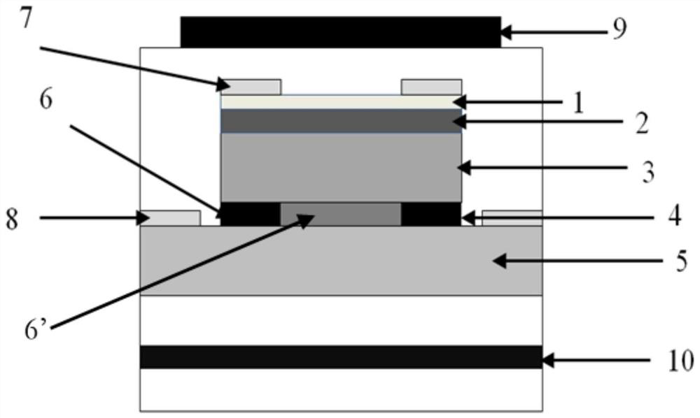
[0022] Such as figure 1 The present invention as shown provides a double-doped resonant cavity single row carrier photodiode, comprising a P-type metal contact layer 1, a diffusion barrier layer 2, an absorption layer 3, a collection layer 4, an N-type metal contact layer 5, an N electrode and The P electrode is provided with a first reflector 9 above the P-type metal contact layer 1. The first reflector 9 has a transmissive surface facing the light incident direction and a reflective surface facing the P-type metal contact layer 1. In the N-type The metal contact layer 5 is provided with a second re...


PUM

PropertyMeasurementUnit
refractive indexaaaaaaaaaa
reflectanceaaaaaaaaaa

Abstract

The invention provides a double-doped resonant cavity uni-traveling carrier photodiode. A device is simultaneously processed in an absorption layer and a collection layer. Linear gradient doping is carried out on the absorption layer, so that the forbidden band width of the absorption layer is linearly changed; or stepped distribution is realized on doped material components of the absorption layer, so that the forbidden band width of the absorption layer is gradiently changed, the built-in electric field intensity of the absorption layer is improved, the electron drift time is shortened, andthe device responsivity is improved. An oxidation process is adopted in the collection layer to obtain a partial oxide insulating layer structure of the collection layer, and due to the low refractiveindex characteristic, the parasitic capacitance of the device is reduced, and the response speed of the device is improved. Besides, a first reflector and a second reflector are introduced to the exterior of the integrated device to form a resonant cavity structure, so that the amplitude of incident signal light in a high-Q-value resonant cavity inner field is enhanced, and the quantum efficiencyof the device is improved.

Description

technical field [0001] The invention belongs to the technical field of semiconductor optoelectronic devices, and in particular relates to a single row carrier photodiode. Background technique [0002] Photodiode (PD) is an important O / E conversion device. It is widely used in the national economy and military fields, and is the core device of application systems such as optical fiber communication, ultra-wideband wireless communication, missile guidance, infrared imaging and remote sensing. Two important indicators of PD are response rate and quantum efficiency. When the photodiode is working, it is difficult to maintain a high response speed when working at a high current density due to the electric field shielding generated by the photogenerated carriers, that is, the space charge effect. Optimizing the external structure to reduce the drift distance of photogenerated carriers and increasing the carrier drift speed to reduce the space charge density of the working device...

Claims


Application Information

Patent Timeline
Patent Type & Authority Applications(China)
IPC IPC(8): H01L31/0232H01L31/0352H01L31/109
CPCH01L31/02327H01L31/109H01L31/035272
Inventor 郝然王三菲甄政汤开达姜华卿石岩金尚忠
Owner CHINA JILIANG UNIV
Why Eureka
Try Eureka