Liquid crystal display with common electrode having cross shaped alignment members
a liquid crystal display and cross-shaped technology, applied in static indicating devices, instruments, non-linear optics, etc., can solve the problems of irregular alignment, narrow angular field of view provided thereby, and take a time in the order of seconds to restor
- Summary
- Abstract
- Description
- Claims
- Application Information
AI Technical Summary
Benefits of technology
Problems solved by technology
Method used
Image
Examples
second embodiment
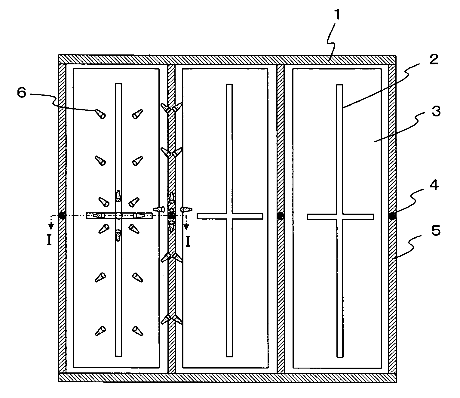
[0077]In the liquid crystal display device of the present invention, while the picture electrode is divided into the three sub-picture electrodes 3A along the signal line 5, it is also possible to divide the picture electrode along a scanning line, or to divide the picture electrode in the vertical and horizontal directions with both lines. The columnar spacer is disposed at a position where it is lapped over the scanning liner or the signal line.
[0078]Next, a liquid crystal display device in a third exemplary embodiment of the present invention is described.
[0079]A basic configuration of the liquid crystal display device of the third embodiment is similar to that of the second embodiment. The third embodiment is different to the second embodiment in that, in the third embodiment, instead of providing a slit on a common electrode, a cross-shaped protruding structure is provided on a common electrode disposed at a position where the common electrode laps over a picture electrode, whi...
first embodiment
[0081]A height of the columnar spacer 4 was adjusted so that, when completing a panel, a cell gap is 4 μm. A position where the columnar spacer 4 is set is described later. Meanwhile, an elastic modulus of the columnar spacer 4 is the same as that in the
[0082]Next, a method of manufacturing a counter substrate, which is a second substrate, is described. A light shielding layer and a color filter are formed on a glass substrate according to a common process. On the color filter layer, the over coat layer of 1μm in thickness is formed using a thermo-set resin. The reason why the over coat layer was formed is to even out unevenness on the color filter layer. An ITO film is formed on the over coat layer using the sputtering technique, thus forming a common electrode. A photosensitive acrylic resin was applied thereon, and dried. This was patterned by using the photolithography technique and the etching technique, forming a cross-shaped protruding structure 2A and a quadrate protruding s...
third embodiment
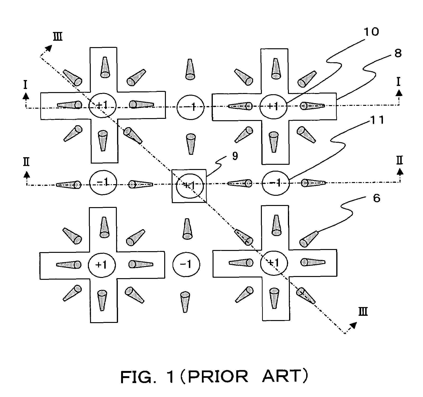
[0087]On the signal line 5, re-aligning of the alignment of the liquid crystal molecules quickly occurs at the singularity of +1 as a base point of the singularity having occurred in the vicinity of the columnar spacer 4 and on the quadrate protruding structure 8. In this manner, an MVA liquid crystal display device can be obtained where re-aligning of the alignment of the liquid crystal molecules quickly occurs even if a pressure is externally applied on a panel. The MVA liquid crystal display device of the present embodiment is applicable not only to a transparent type but also to a semitransparent MVA liquid crystal display device. Furthermore, in the above third embodiment of the present invention, the columnar spacer 4 can be placed on the counter substrate instead of on the TFT substrate.
[0088]In the liquid crystal display device of the above third embodiment of the present invention, instead of the slit 2, the cross-shaped protruding structure may be provided on the common el...
PUM
| Property | Measurement | Unit |
|---|---|---|
| width | aaaaa | aaaaa |
| width | aaaaa | aaaaa |
| angle | aaaaa | aaaaa |
Abstract
Description
Claims
Application Information


