Model-based measurement of semiconductor device features with feed forward use of data for dimensionality reduction

a semiconductor device and feature technology, applied in the direction of distance measurement, instruments, testing circuits, etc., can solve the problems of prohibitively long processing time to a solution, prohibitively large number of pre-calculated solutions, and substantially more difficult and/or time-consuming measurement using scatterometry, etc., to reduce the dimensionality of a feature model

Active Publication Date: 2010-05-11
KLA TENCOR TECH CORP
View PDF10 Cites 24 Cited by
  • Summary
  • Abstract
  • Description
  • Claims
  • Application Information

AI Technical Summary

Benefits of technology

[0012]The present application discloses a new technique which reduces the dimensionality of a feature model by re-use of data that has been obtained by a prior measurement. The data re-used from the prior measurement may range from parameters, such a

Problems solved by technology

In practice, as the number of parameters in the model increases, the measurement using scatterometry becomes substantially more difficult and/or time consuming.
Unfortunately, using such a library mode, the number of pre-calculated solutions becomes prohibitively large as the number of parameters becomes large.
Alternatively, in a real-time regression mode of performing scatterometry, the processing time to a solution becomes prohibitively long as the number of parameters becomes large.
However, that approach is costly and limited in that th

Method used


Image

  • Model-based measurement of semiconductor device features with feed forward use of data for dimensionality reduction
  • Model-based measurement of semiconductor device features with feed forward use of data for dimensionality reduction
  • Model-based measurement of semiconductor device features with feed forward use of data for dimensionality reduction

Examples


Embodiment Construction

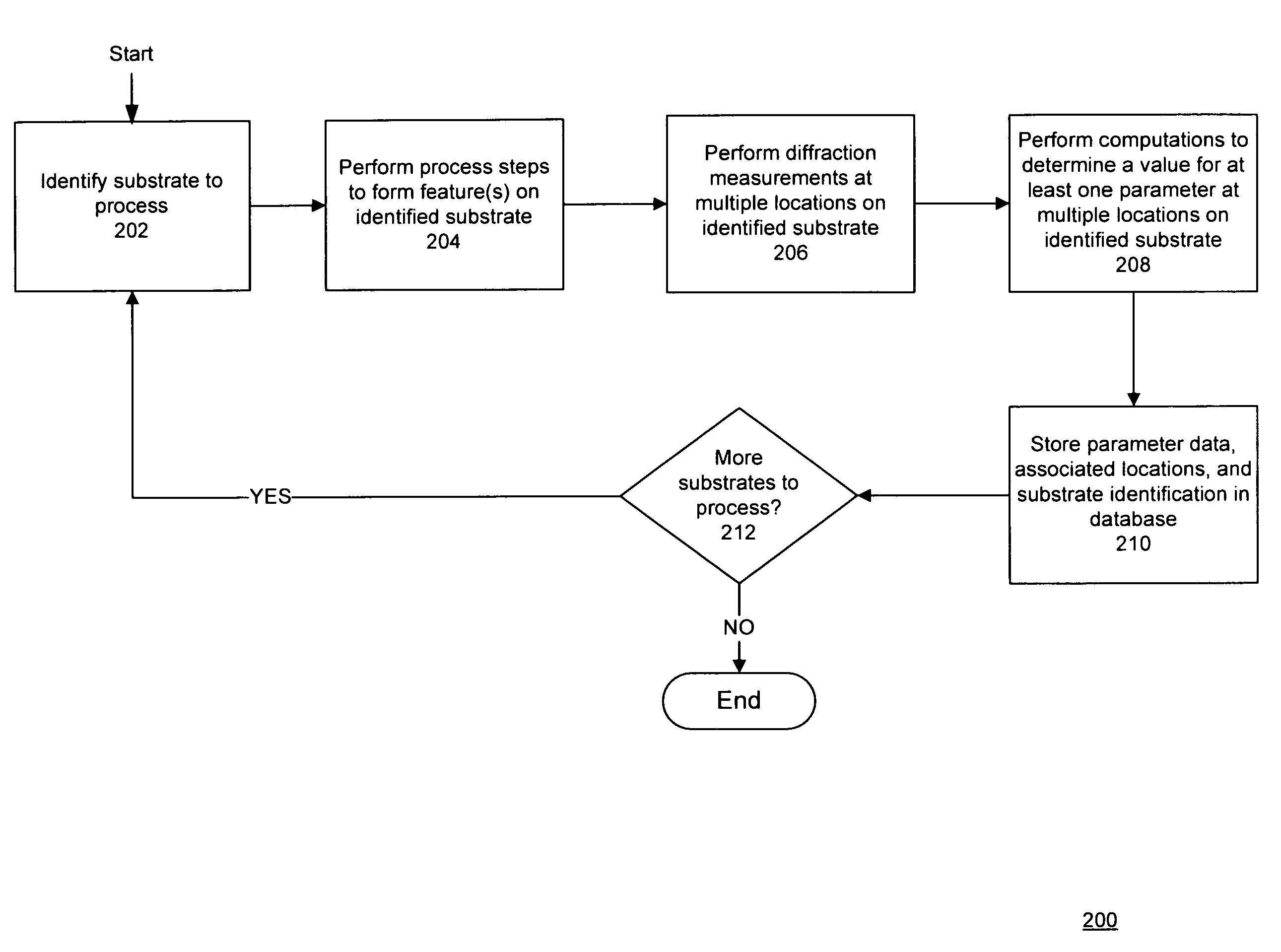
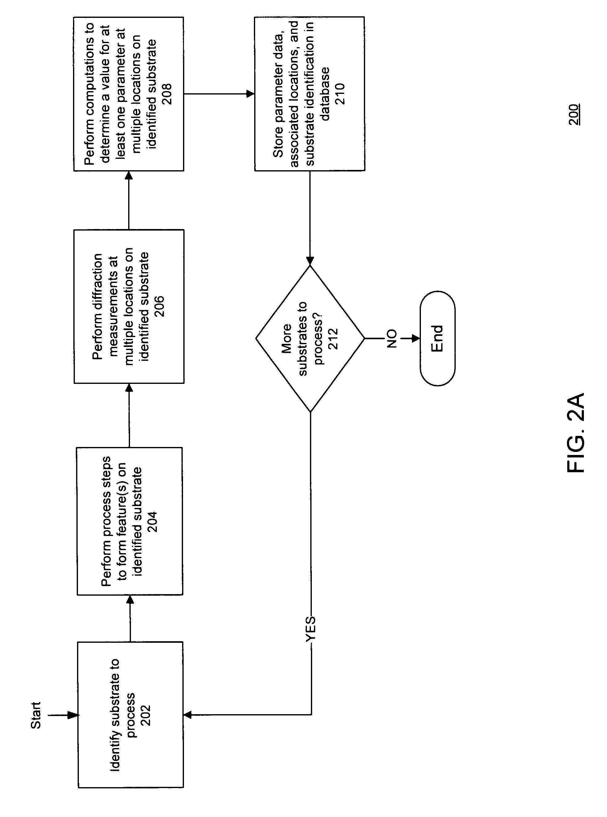
[0018]As described below, the present application discloses a new technique which reduces the dimensionality of a feature model by re-use of data that has been obtained by a prior measurement. The data re-used from the prior measurement may range from parameters, such as geometrical dimensions, to more complex data that describe the electromagnetic scattering function of an underlying layer (for example, a local solution of the electric field properties).

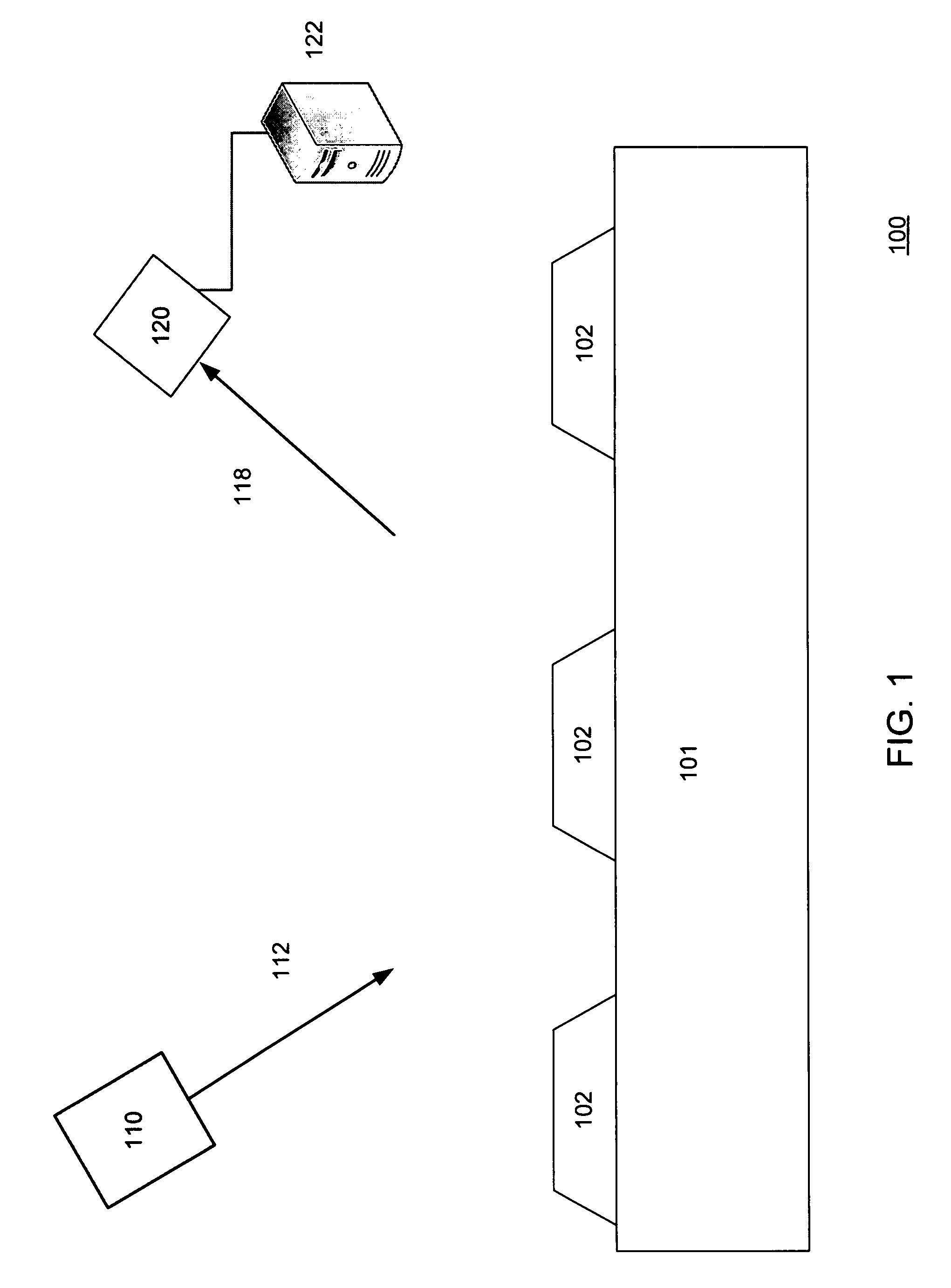
[0019]In accordance with an embodiment of the invention, there is a need for specific procedures to obtain the relevant data from the pertinent source, to forward the relevant data, and to use the forwarded data to reduce the dimensionality of the computation of a current scatterometry measurement. The elements of a system to implement this feed forwarding of data may include: a means to determine the optimal source of the prior data; a means to collect and process the prior data and to store it in a database when required; a means ...


PUM


Abstract

The present application discloses a new technique which reduces the dimensionality of a feature model by re-use of data that has been obtained by a prior measurement. The data re-used from the prior measurement may range from parameters, such as geometrical dimensions, to more complex data that describe the electromagnetic scattering function of an underlying layer (for example, a local solution of the electric field properties).

Description

TECHNICAL FIELD[0001]1. Background of the Invention[0002]The present disclosure relates to apparatus and methods for inspecting and analyzing semiconductor wafers and other substrates using scatterometry and related techniques.[0003]2. Description of the Background Art[0004]Scatterometry refers to an optical technique that analyzes diffraction to deduce structural details of a diffracting sample. The diffracting sample is generally a periodic structure, that is, a grating. Scatterometry may be used to measure or analyze two-dimensional structures (line gratings), as well as three-dimensional structures (such as periodic patterns of mesas or vias on a substrate).[0005]Metrology methods using scatterometry rely on being able to accurately model the features that are being measured, calculate the light diffraction properties of the feature, and find a match between the calculated and measured values. In other words, theoretical model is defined for each physical structure to be analyze...

Claims


Application Information

Patent Timeline
IPC IPC(8): G01R27/28
CPCG01N21/956G01N21/4788
Inventor WACK, DANIEL C.VELDMAN, ANDREIRATNER, EDWARD R.HENCH, JOHNBAREKET, NOAH
Owner KLA TENCOR TECH CORP
Why Eureka
Try Eureka