Unlock instant, AI-driven research and patent intelligence for your innovation.

Multi-bit memory device having resistive material layers as storage node and methods of manufacturing and operating the same

a resistive material and memory device technology, applied in semiconductor devices, digital storage, instruments, etc., can solve the problems of reducing the current supply capability, difficult operation of the pram, and restricting the integration density of the pram, so as to reduce the restriction on the integration density

Active Publication Date: 2010-05-18
SAMSUNG ELECTRONICS CO LTD
View PDF25 Cites 26 Cited by
  • Summary
  • Abstract
  • Description
  • Claims
  • Application Information

AI Technical Summary

Benefits of technology

The present invention provides a resistive memory device with high integration density and low driving voltage, and can write at least 2-bit data. The device includes a substrate, a transistor, and a storage node, which includes a lower electrode, a first phase change layer, a first barrier layer, a second phase change layer, and an upper electrode. The method of manufacturing the device includes forming a contact hole exposing one of the first and second impurity regions in the first interlayer insulating layer, filling the contact hole with a conductive plug, and sequentially forming layers of the first through third phase change layers and the first barrier layer. The method of operating the device includes applying a write voltage between the upper and lower electrodes of the storage node to cause a phase change of the second phase change layer. The device can offer high data storage capacity and low power consumption.

Problems solved by technology

However, the phase change current applied to change a portion of the GST layer 22 to the amorphous state poses a major challenge to improving the characteristics of PRAM.
However, as the transistor becomes smaller, its current supply capability decreases.
Thus, when the current allowed through the transistor is less than that needed to cause the phase change of the GST layer 22, the PRAM is difficult to operate.
This results in a restriction to the integration density of PRAM.
Another drawback of the conventional PRAM is that it cannot write more than 2-bit data.

Method used


Image

  • Multi-bit memory device having resistive material layers as storage node and methods of manufacturing and operating the same
  • Multi-bit memory device having resistive material layers as storage node and methods of manufacturing and operating the same
  • Multi-bit memory device having resistive material layers as storage node and methods of manufacturing and operating the same

Examples


Embodiment Construction

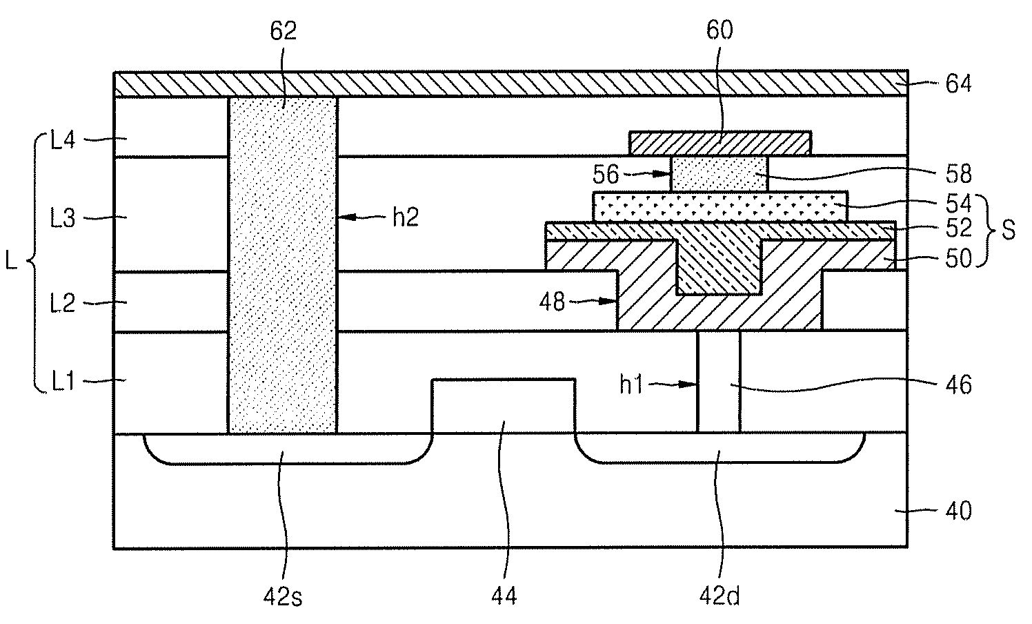
[0033]A multi-bit memory device having resistive material layers as a storage node and methods of manufacturing and operating the same according to embodiments of the present invention will now be described more fully with reference to the accompanying drawings. In the drawings, the thicknesses of layers and regions are exaggerated for clarity.

[0034]FIG. 2 shows the configuration of a multi-bit memory device according to an embodiment of the present invention. Referring to FIG. 2, first and second impurity regions 42s and 42d are formed in a substrate 40 such that the impurity regions 42s and 42d are doped with impurities of an opposite conductivity type to that of the substrate 40. The substrate 40 may be either p- or n-type semiconductor. The first and second impurity regions 42s and 42d are spaced apart from each other and used respectively as a source region and a drain region. However, the functions of the first and second impurity regions 42s and 42d may alternatively be the r...


PUM


Abstract

Provided are a multi-bit memory device having resistive material layers as a storage node, and methods of manufacturing and operating the same. The memory device includes a substrate, a transistor formed on the substrate, and a storage node coupled to the transistor, wherein the storage node includes: a lower electrode connected to the substrate; a first phase change layer formed on the lower electrode; a first barrier layer overlying the first phase change layer; a second phase change layer overlying the first barrier layer; and an upper electrode formed on the second phase change layer.

Description

CROSS-REFERENCE TO RELATED PATENT APPLICATION[0001]This application claims the benefit of Korean Patent Application No. 10-2005-0028544, filed on Apr. 6, 2005, in the Korean Intellectual Property Office, the disclosure of which is incorporated herein in its entirety by reference.BACKGROUND OF THE INVENTION[0002]1. Field of the Invention[0003]The present invention relates to a semiconductor memory device and a method of manufacturing and operating the same, and more particularly, to a multi-bit memory device having resistive material layers as a storage node, and methods of manufacturing and operating the same.[0004]2. Description of the Related Art[0005]There are two types of memory: volatile memory, that loses the stored data when power is turned off, and non-volatile memory, that does not require power to retain its contents. With the advancement in Internet technology and increasing popularity of mobile communication devices, increasing attention is being directed toward non-vola...

Claims


Application Information

Patent Timeline
Patent Type & Authority Patents(United States)
IPC IPC(8): H01L45/00G11C11/56H10B69/00
CPCG11C11/56G11C11/5678G11C13/0004H01L27/2436H01L45/1675H01L45/12H01L45/1233H01L45/144H01L45/146H01L45/06H10B63/30H10N70/801H10N70/231H10N70/8828H10N70/8833H10N70/063H10N70/826
Inventor LEE, JUNG-HYUN
Owner SAMSUNG ELECTRONICS CO LTD
Features
  • R&D
  • Intellectual Property
  • Life Sciences
  • Materials
  • Tech Scout
  • Unparalleled Data Quality
  • Higher Quality Content
  • 60% Fewer Hallucinations
Learn More