Method for manufacturing single sided substrate

a manufacturing method and single-sided technology, applied in the field of single-sided circuit boards, can solve the problems of inability to easily raise the density at which elements are mounted, the manufacturing process becomes too complicated, and the multi-layer printed circuit board structure cannot easily address the needs of considerable reductions in the size of portable electronic devices, etc., to achieve the effect of reducing the height and diameter of each projecting conductor, reducing the number of projecting conductors, and reducing the height and diameter of each proj

Inactive Publication Date: 2010-05-25
IBIDEN CO LTD
View PDF49 Cites 6 Cited by
  • Summary
  • Abstract
  • Description
  • Claims
  • Application Information

AI Technical Summary

Benefits of technology

[0038]These single-sided circuit boards are laminated to other substrates through an adhesive layer and are integrated by the heat pressing. Therefore, inspection for detecting whether or not the conductive circuit or the like has a defective portion can be performed before the single-sided circuit boards are laminated. Hence it follows that only single-sided circuit boards free from any defect can be used in the laminating process. That is, the manufacturing method is able to reduce defects in the manufacturing process. As a result, the multilayer printed circuit board having the IVH structure can be manufactured with a high manufacturing yield.
[0046]In the single-sided circuit board according to the present invention, the projecting conductors are formed on the via holes filled with the electrolytic plating. Therefore, electrical connection between the upper and lower conductive layers in the multilayer printed circuit substrate can be easily established by penetrating the relatively thin organic adhesive layer. Therefore, the height and the diameter of each projecting conductor can be reduced. Hence it follows that the pitch between adjacent projecting conductors can be shortened. Therefore, the pitch between adjacent via holes can also be shortened. As a result, addressing to the raising of the density can be permitted. Since the via holes are filled with the electrolytic plating, the resistance value between the upper and the lower conductor layers can be lowered.

Problems solved by technology

Therefore, the density at which elements are mounted cannot be easily raised.
As a result, there arises a problem in that the multilayer printed circuit board having the through hole structure cannot easily address needs for considerable reductions in the sizes of the portable electronic apparatuses, realizing narrow pitch packages and practical use of MCM.
Therefore, the manufacturing process becomes too complicated and considerable time is required to complete the manufacturing operation.
If the multilayer printed circuit board having the IVH structure which can be obtained by the above-mentioned manufacturing method encounters only one defective portion (only one defective process) in the patterning operation during the manufacturing process, the overall circuit board, which is the final product, becomes a defective product Hence it follows that the manufacturing yield deteriorates excessively.

Method used


Image

  • Method for manufacturing single sided substrate
  • Method for manufacturing single sided substrate
  • Method for manufacturing single sided substrate

Examples


Embodiment Construction

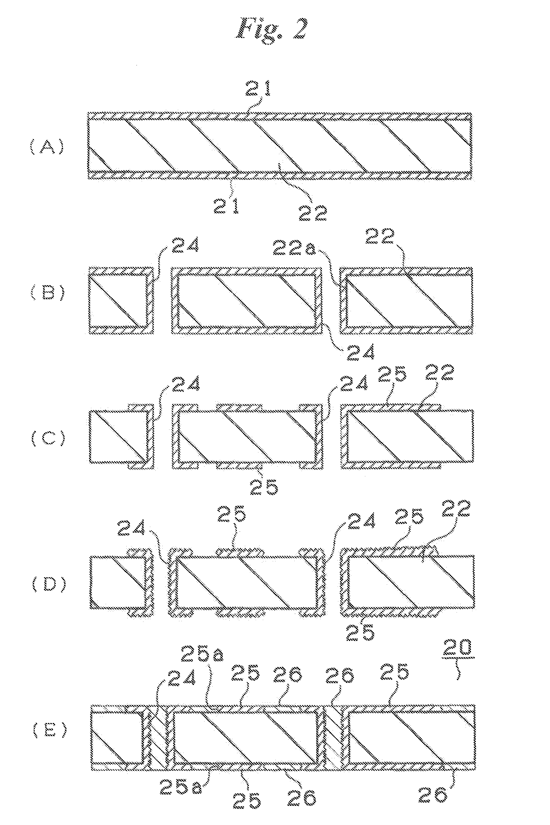
[0057]A single-sided circuit board and a multilayer printed circuit board and a manufacturing method therefor used single-sided circuit board according to an embodiment of the present invention will now be described with reference to the drawings.

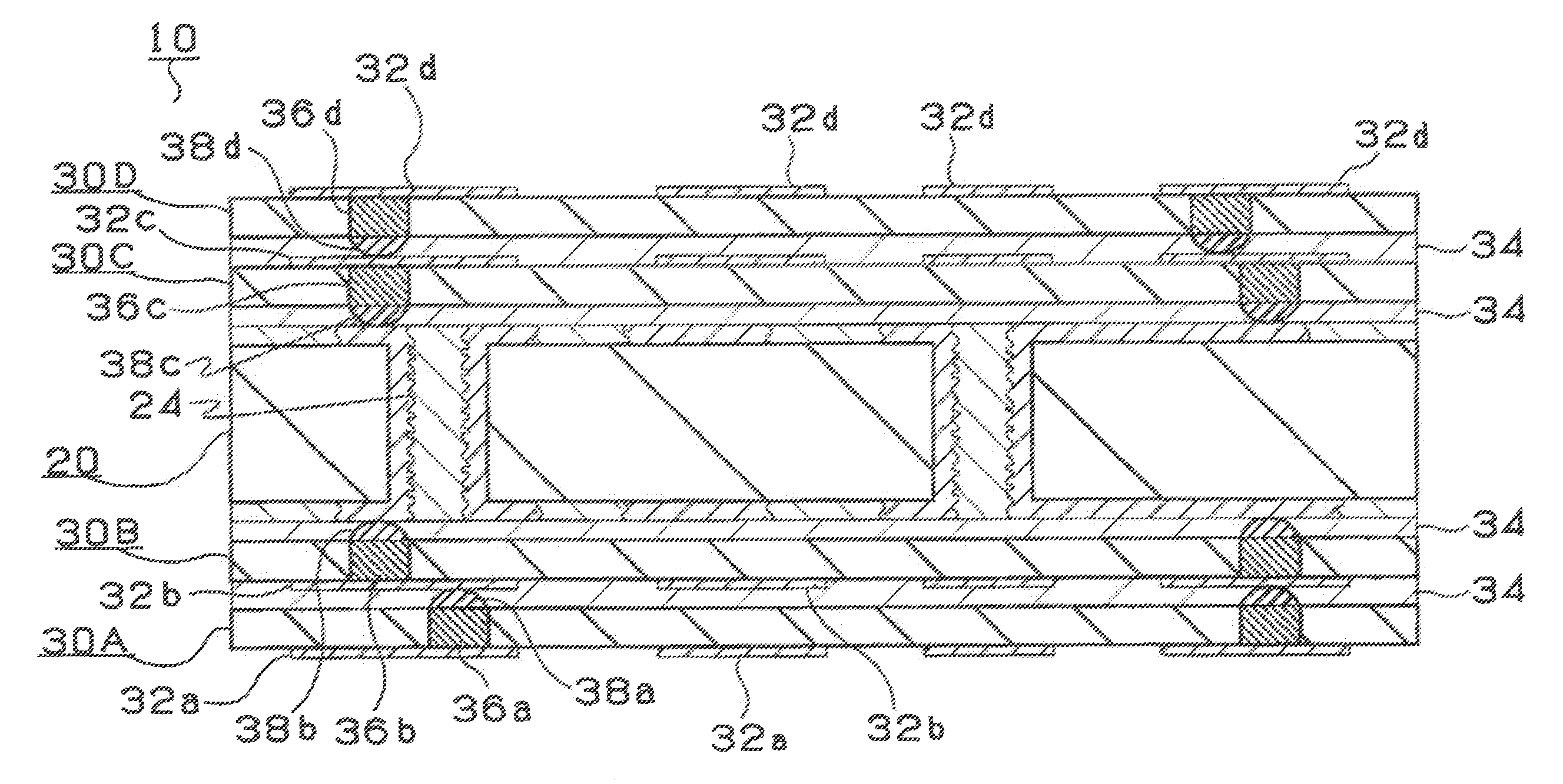
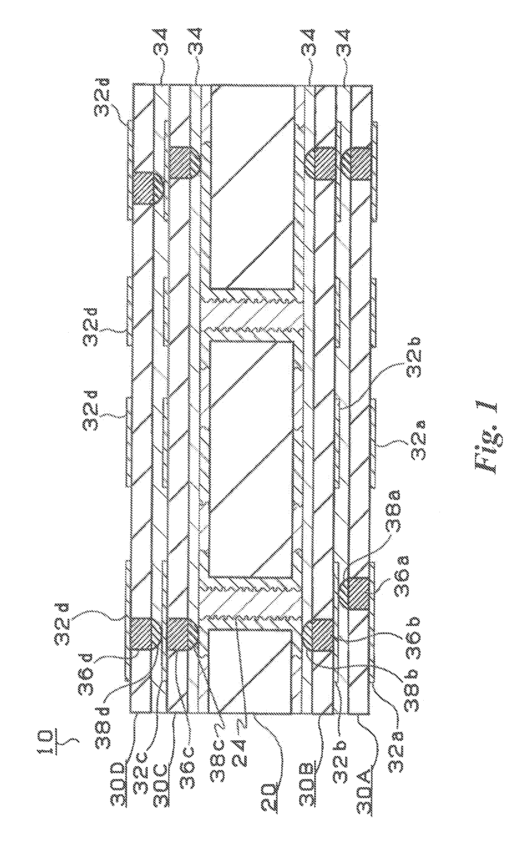
[0058]FIG. 1 shows a vertical cross section of a multilayer printed circuit board having a full-thickness IVH structure. A multilayer printed circuit board 10 is a multilayer printed circuit board incorporating a core substrate 20 disposed in a central portion of the multilayer printed circuit board 10 and single-sided circuit boards 30A, 30B, 30C and 30D of the present invention, two substrates of which are formed on the upper surface of the core substrate 20 and the lower surface of the same, respectively.

[0059]Conductive circuits 32a, 32b, 32c and 32d each having a predetermined pattern are formed on the surfaces of the corresponding single-sided circuit boards 30A, 30B, 30C and 30D. Adhesive layers 34 are formed on other surfaces of the...


PUM

PropertyMeasurementUnit
thicknessaaaaaaaaaa
thicknessaaaaaaaaaa
thicknessaaaaaaaaaa

Abstract

Holes (40a) are formed with a laser beam through an insulating substrate (40) on which a metallic layer (42) is formed and via holes (36a) are formed by filling up the holes (40a) with a metal (46). After the via holes (36a) are formed, a conductor circuit (32a) is formed by etching the metallic layer (42) and a single-sided circuit board (30A) is formed by forming projecting conductors (38a) on the surfaces of the via holes (36a). The projecting conductors (38a) on the circuit board (30A) are put on the conductor circuit (32b) of another single-sided circuit board (30B) with adhesive layers (50) composed of an uncured resin in-between and heated and pressed against the circuit (32b). The projecting conductors (38a) get in the uncured resin by pushing aside the resin and are electrically connected to the circuit (32b). Since single-sided circuit boards (30A, 30B, 30C, and 30D) can be inspected for defective parts before the boards (30A, 30B, 30C, and 30D) are laminated upon one another, only defectless single-sided circuit can be used in the step of lamination.

Description

BACKGROUND OF THE INVENTION[0001]1. Field of the Invention[0002]The present invention relates to a single-sided circuit board and a manufacturing method therefor, and more particularly to a single-sided circuit board used for manufacture of a multilayer printed circuit board having an interstitial via hole (IVH) structure and a manufacturing method therefor.[0003]2. Description of the Related Art[0004]A conventional multilayer printed circuit board is constituted by a laminate obtained by alternately laminating copper-clad laminates and prepregs. The laminate has a surface on which a surface wiring pattern has been formed. Moreover, an internal wiring pattern is formed between interlayer insulating layers. Through holes are, by punching formed in the direction of the thickness of the laminate to establish the electric connections among internal wiring patterns or among internal wiring patterns and the surface wiring patterns.[0005]The multilayer printed circuit board having the abov...

Claims


Application Information

Patent Timeline
Patent Type & Authority Patents(United States)
IPC IPC(8): H01K3/10H05K3/00H05K3/28H05K3/38H05K3/42H05K3/46
CPCH05K3/4617H05K3/0035Y10T29/49155H05K3/382H05K3/386H05K3/423H05K3/4602H05K3/4652H05K2201/0195H05K2201/035H05K2201/0394H05K2201/09563H05K2203/0733H05K2203/1189Y10T29/49126Y10T29/49128Y10T29/49117Y10T29/49165H05K3/28
Inventor ENOMOTO, RYOHIRAMATSU, YASUJI
Owner IBIDEN CO LTD
Why Eureka
Try Eureka