Ge photodetectors

a photodetector and photoelectric technology, applied in the field of photodetectors, can solve problems such as increasing reverse leakage currents

Inactive Publication Date: 2010-05-25
MASSACHUSETTS INST OF TECH
View PDF8 Cites 23 Cited by
  • Summary
  • Abstract
  • Description
  • Claims
  • Application Information

AI Technical Summary

Benefits of technology

[0007]According to another aspect of the invention, there is provided a method of forming a photodiode. The method includes forming a base that comprises Ge, and forming a collector that comprises Si. The base and collector form a Si / Ge heterojunction allowing the unpinning of Fermi energy level (EF) of the photodiode.
[0008]According to another aspect of the invention, there is provided a phototransistor. The phototransistor includes an emitter and a base that comprises Ge. A collector comprises Si. The base, emitter, and collector form at least one Si / Ge heterojunction allowing the unpinning of Fermi energy level (EF) of the phototransistor.
[0009]According to another aspect of the invention, there is provided method of forming a phototransistor. The method includes forming an emitter and forming a base that comprises Ge. A collector is formed that comprises Si. The base, emitter, and collector form at least one Si / Ge heterojunction allowing the unpinning of Fermi energy level (EF) of the phototransistor.

Problems solved by technology

However, breakdown voltage VBR is lower in narrow gap semiconductors which increases reverse leakage currents.

Method used


Image

  • Ge photodetectors
  • Ge photodetectors
  • Ge photodetectors

Examples


Embodiment Construction

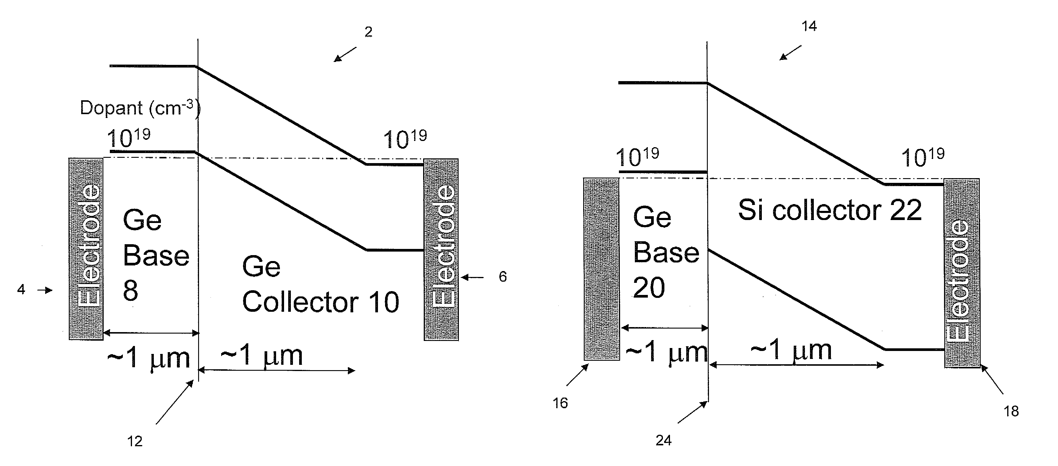
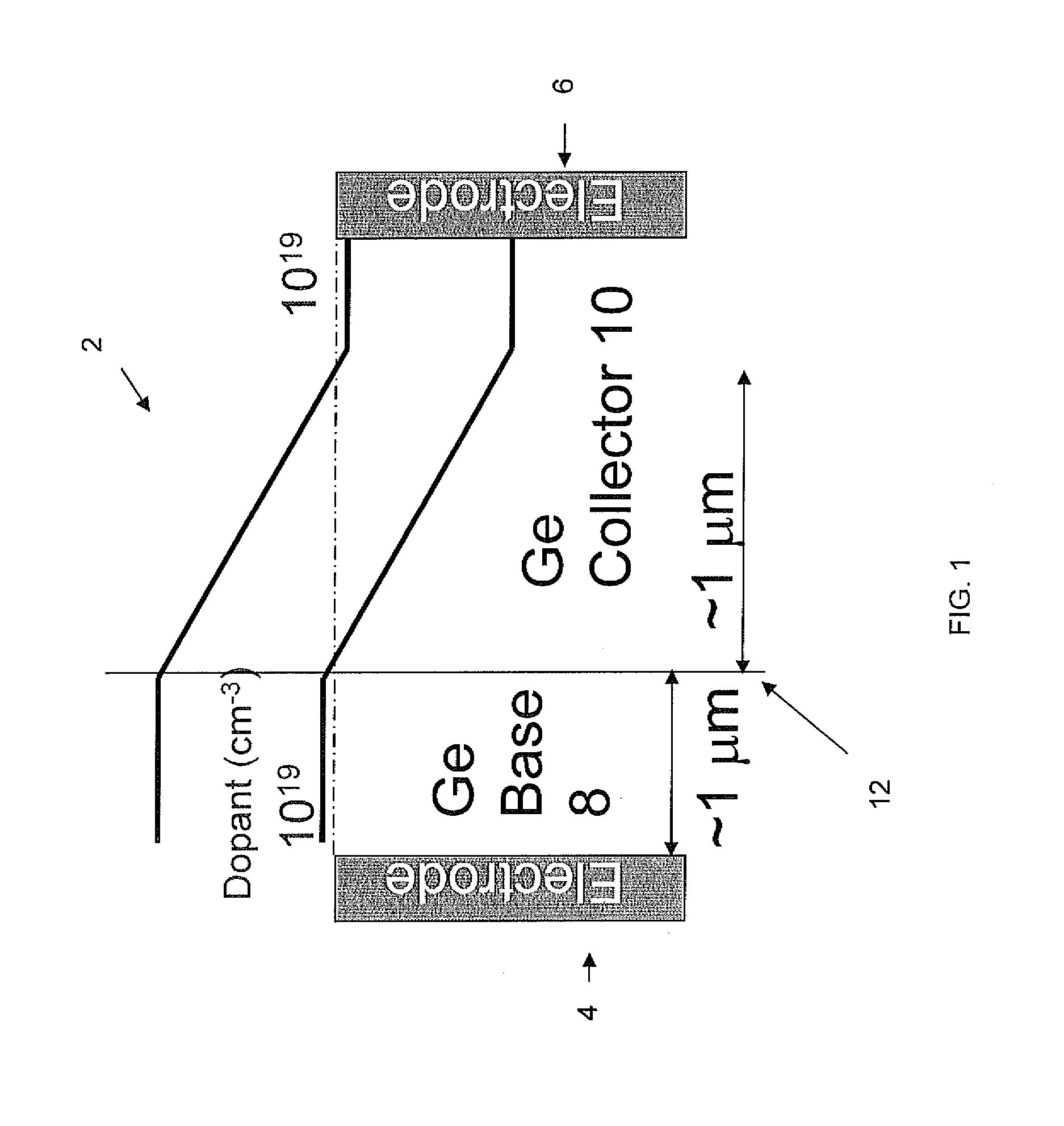
[0020]FIG. 1 illustrates the operations of a Ge Hetero pin Photodiode 2. The photodiode 2 includes two electrodes 4 and 6, a Ge base 8, and a Ge collector 10. The Ge base 8 is sized at ˜1 μm from the electrode 4 to the Si junction 12. The Ge collector 10 is sized at ˜1 μm from the junction 12 to the electrode 6 to form a pn junction. Note the Ge base 8 has a higher electron concentration then the Ge collector 10.

[0021]Higher electric field application is generally necessary for photodetectors to achieve higher responsitivity. However, the breakdown voltage (VBR) is lower in narrow band gap semiconductors which increases reverse leakage currents. Thus, high field application is hard in photodetectors with similar bandgap Ge.

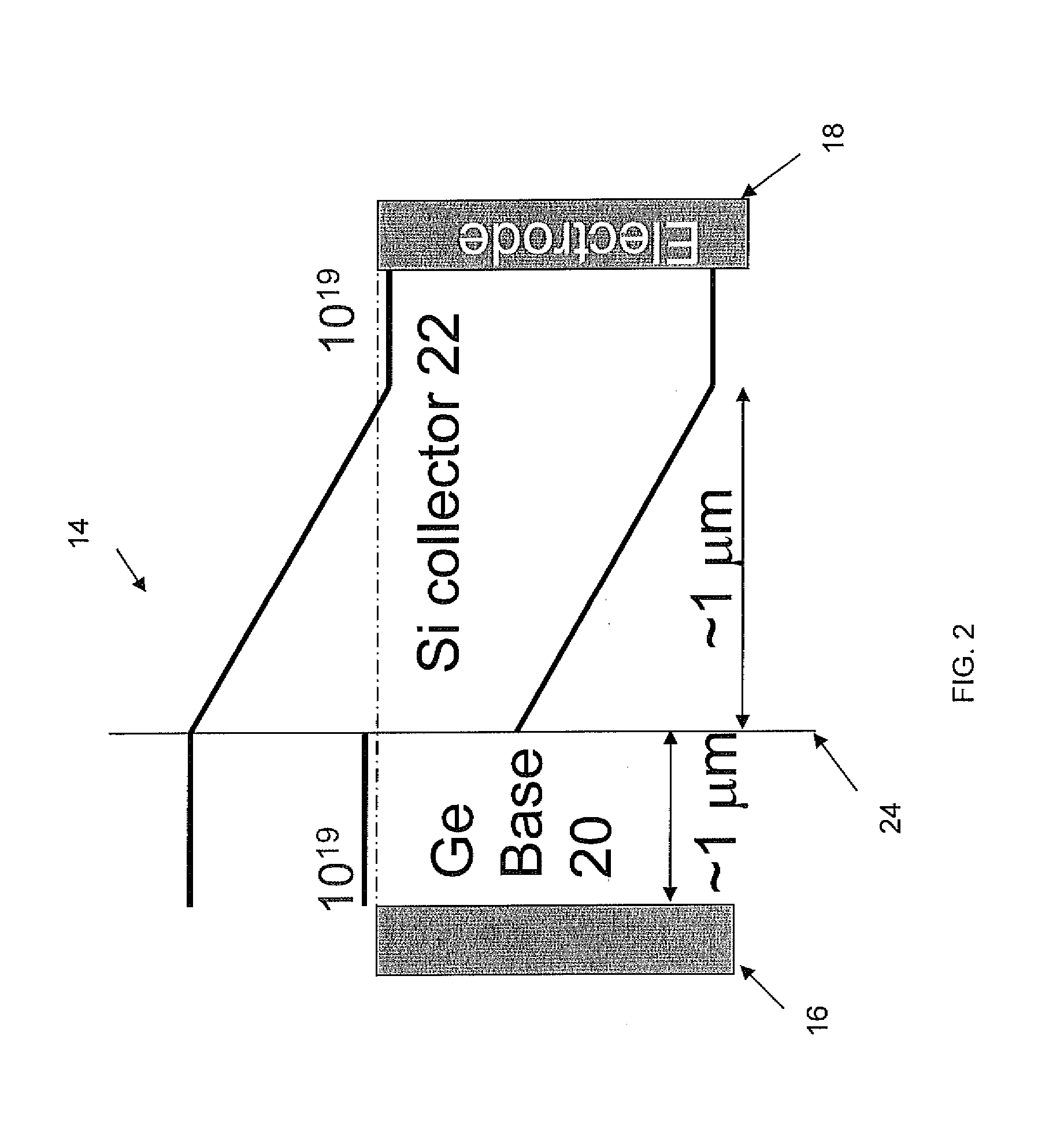
[0022]FIG. 2 illustrates the operations of a Ge / Si hetero pin photodiode 14. The photodiode 14 includes two electrodes 16 and 18, a Ge base 20, and a Si collector 22. The Ge base 20 is sized at ˜1 μm from the electrode 16 to the Ge / Si heterojunction 24. The Si col...


PUM


Abstract

A phototransistor includes an emitter and a base that comprises Ge. A collector comprises Si. The base, emitter, and collector form at least one Si / Ge heterojunction allowing the unpinning of Fermi energy level (EF) of the phototransistor.

Description

PRIORITY INFORMATION[0001]This application claims priority from provisional application Ser. No. 60 / 591,769 filed Jul. 28, 2005.BACKGROUND OF THE INVENTION[0002]The invention relates to the field of photodetectors, in particular photodetectors having higher breakdown voltages.[0003]Photodetectors are fundamental devices that convert optical signals into electric signals. Fiber optical communication employs 1300 and 1550 nm wavelengths because of low attenuation coefficients of silica fibers. Er doped fiber amplifiers emphasize the importance of 1550 nm because of the direct amplification of optical signals without converting to electric signals. The amplification range between 1530-1560 nm is referred to as C-band, and the recently extended amplification range between 1570-1608 nm is referred to as L-band. The photodetectors for 1550 nm detection have so far been InGaAs photodetectors, since InGaAs is a direct semiconductor whose bandgap is 0.75 eV (corresponding to 1653 nm). Thus, ...

Claims


Application Information

Patent Timeline
Patent Type & Authority Patents(United States)
IPC IPC(8): H01L29/737
CPCH01L31/028H01L31/0312H01L31/109H01L31/1105H01L31/1055Y02E10/547
Inventor WADA, KAZUMIKIMERLING, LIONEL C.
Owner MASSACHUSETTS INST OF TECH
Why Eureka
Try Eureka