Data processor

a data processor and data technology, applied in the field of data processors, can solve problems such as the inability to avoid deterioration in data transfer performance, and achieve the effect of enhancing data transfer performan

Inactive Publication Date: 2010-05-25
RENESAS ELECTRONICS CORP
View PDF16 Cites 1 Cited by
  • Summary
  • Abstract
  • Description
  • Claims
  • Application Information

AI Technical Summary

Benefits of technology

[0005]The inventor investigated an access control configuration for causing a memory having a static RAM interface to carry out a burst operation. More specifically, in the case in which an access exceeding an address range corresponding to a storage capacity of a burst buffer is to be carried out, it is necessary to read data from a memory array plural times. Accordingly, it is necessary to take a start address of the burst operation into consideration in order to set a frequency of a burst. For example, a data bus width is set to be 16 bits and a size of the burst buffer is set to be 8 words (16 bytes). By fixing high order addresses A4 to Ax (x is an optional integer of 5 or more) and changing 3 bits of low order addresses A1 to A3, it is possible to select data in the burst buffer in 1-word (16-bit) unit, thereby carrying out a burst access. In the case in which a start address of the burst access is H′00, it is possible to give a burst access continuously eight times up to data D0 to D7 by changing a sequential address in order of H′02, H′04, H′06, H′08, H′0A, H′0C and H′0E. In this case, it is preferable to set the frequency of the burst to be eight at a maximum for a memory controller. When the start address of the burst operation is H′08 through the setting, however, data after H′10 provided across a boundary of the burst buffer are not output in an expected timing if the sequential address is changed in order of H′08, H′0A, H′0C, H′0E, H′10, H′12, H′14 and H′16. The reason is as follows. When the address is changed from H′0E to H′10 (a fourth bit of the address is changed), the memory recognizes a first access of the burst operation and a data read from the memory array to the burst buffer is generated so that the data cannot be output in an expected access time. In order to prevent such a drawback from being caused, it is possible to propose that a burst access to be started in a middle address such as the address H′08 is prohibited in software so as to prevent a burst access from being given across a boundary of the burst buffer or a value of the frequency of the burst which can be set to the memory controller is limited to be four or less, for example, so as to freely output the expected data in a permitted start address of H′00 and H′08. However, it is impossible to avoid a deterioration in a data transfer performance through a memory access by any method.
[0006]It is an object of the invention to provide a data processor capable of enhancing a data transfer performance through a burst access together with a memory.
[0009][1] A data processor has a central processing unit, and a memory controller (6) capable of controlling a memory (8) to be connected to an outside. The memory has a buffer (25) capable of temporarily holding data within an address range corresponding to a predetermined bit number on a low order side of an address signal and is caused to freely carry out a burst operation for inputting / outputting data by a data transfer between the buffer and the outside for an access request in which an access address is changed within the address range. The memory controller carries out a predetermined access control capable of continuously performing the burst operation of the memory if an access exceeding the address range is detected when the memory is caused to carry out the burst operation, thereby giving the access. When the memory controller gives the burst access to the memory, consequently, the access control capable of continuously carrying out the burst operation of the memory is performed if the access exceeding the address range is detected. Therefore, it is possible to enhance a data transfer performance through a burst access without requiring to restrict a burst access exceeding the address range or to limit the frequency of the burst.
[0011]In another specific configuration according to the invention, when detecting the access exceeding the address range, the memory controller carries out a control for extending an output period of the address for the memory, thereby causing the burst operation of the memory to be freely executed continuously. The control for extending the output period of the address serves to maintain a time required for updating data of the buffer when responding to a read request, for example. Consequently, it is possible to wait for an output of expected data. Furthermore, it is also possible to carry out a control for delaying a data output timing from the buffer through an output enable signal simultaneously with the control for extending the output period of the address. The control serves to maintain a time required for transferring the data of the buffer to a writing system circuit when responding to a write request. It is possible to wait for a completion of a data transfer for preventing write data held in the writing system circuit from being undesirably overwritten by write data transferred internally from the buffer.
[0014][2] A data processor according to another aspect has a memory controller capable of controlling a memory to be connected to an outside. The memory has a memory array and a buffer capable of temporarily holding data read from the memory array within an address range corresponding to a predetermined bit number on a low order side of an address signal, and it is possible to carry out a burst reading operation for outputting, from the buffer to the outside, data to meet a read access request in which an access address is changed within the address range when the data are held in the buffer. When causing the memory to carry out the burst reading operation, the memory controller performs a control for maintaining a necessary period of time for updating the data of the buffer by a memory operation responding to a read request exceeding the address range and thus executes the burst reading operation of the memory continuously if it detects the read request. When the memory controller gives a burst read access to the memory, consequently, the access control capable of continuously carrying out the burst reading operation of the memory is performed if an access exceeding the address range is detected. Consequently, it is possible to enhance a data transfer performance through a burst access without requiring to restrict a burst read access exceeding the address range or to limit the frequency of the burst.
[0015][3] A data processor according to a further aspect has a memory controller capable of controlling a memory to be connected to an outside. The memory has a memory array and a buffer capable of temporarily holding data read from the memory array within an address range corresponding to a predetermined bit number on a low order side of an address signal, and information stored in an address specified by an address signal can be output to the outside after a predetermined access time in response to an input of the address signal. When detecting a read request exceeding the address range of data held in the buffer, the memory controller carries out an access control for maintaining a necessary period of time for updating the data of the buffer by a memory operation in response to the read request. When there is provided a static RAM interface capable of outputting stored information to an outside after a predetermined access time in response to the input of the address signal, a selection in the memory array has no change if the access is continuously given within the range of the data held in the buffer. Therefore, it is possible to read necessary data in a short access cycle. By maintaining a period of time required for internally transferring the data selected in the memory array into the buffer in response to a read request exceeding the address range, subsequently, it is possible to continuously carry out an operation for reading the necessary data in the short access cycle.

Problems solved by technology

However, it is impossible to avoid a deterioration in a data transfer performance through a memory access by any method.

Method used


Image

  • Data processor
  • Data processor
  • Data processor

Examples


Embodiment Construction

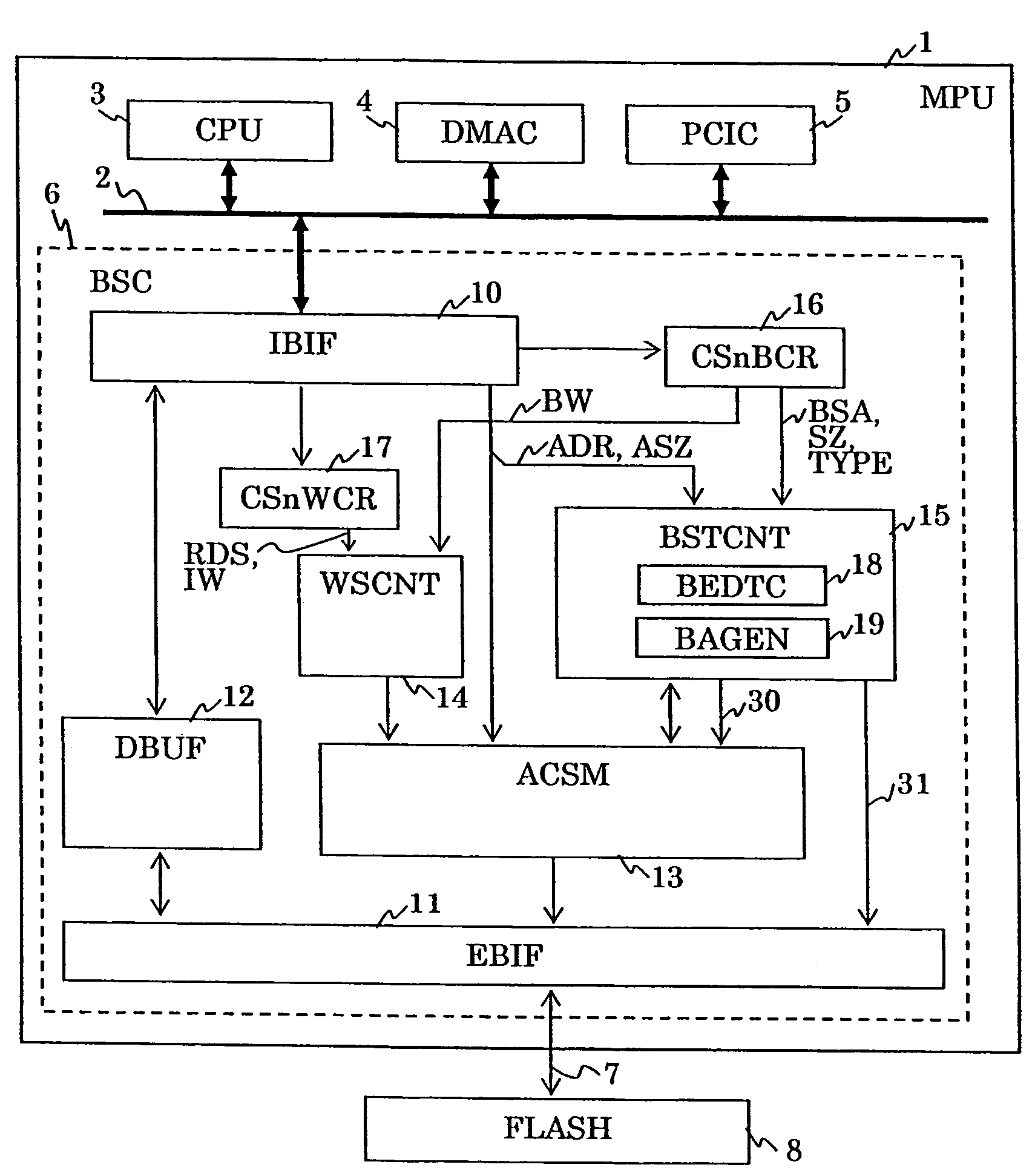
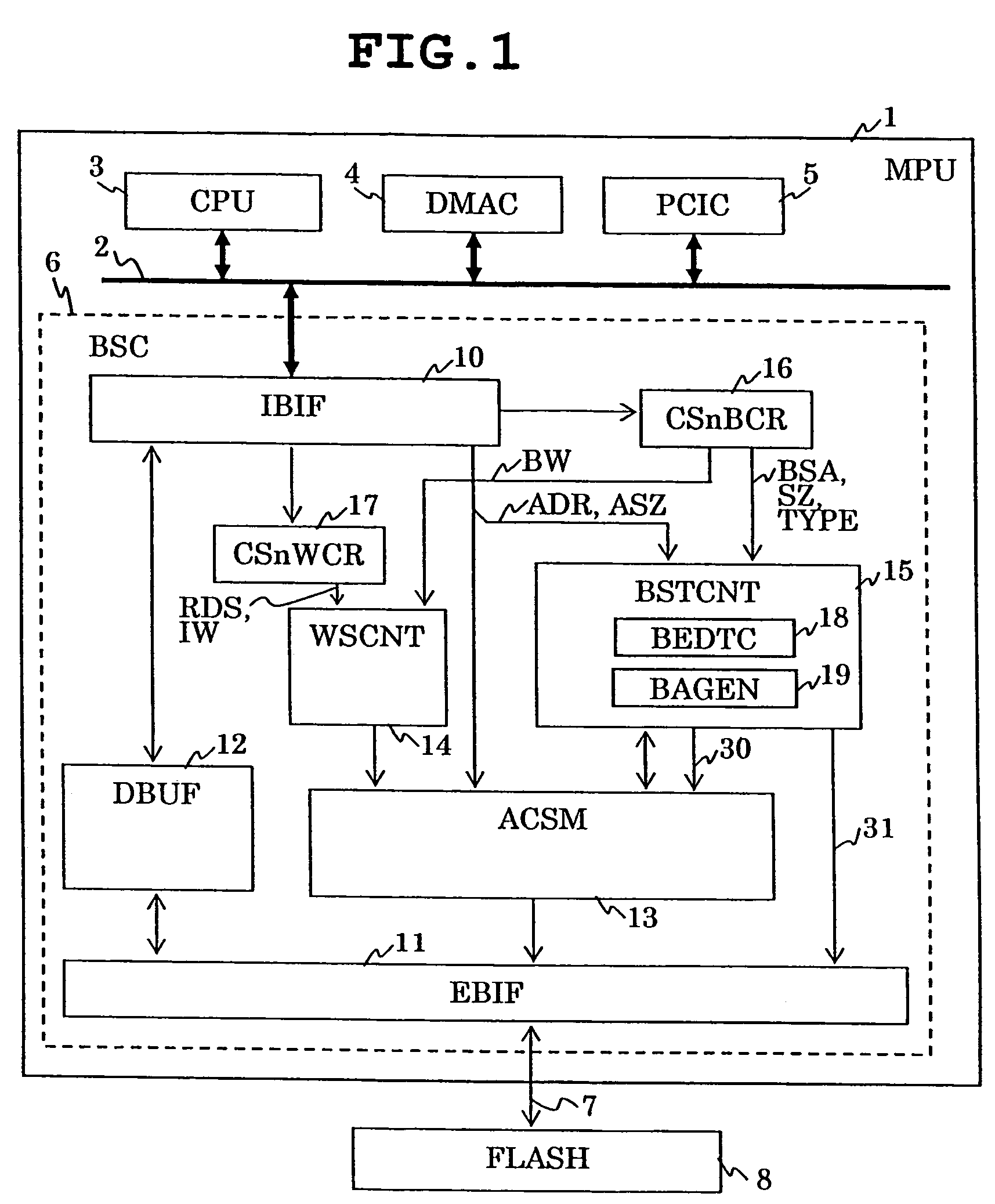
[0029]FIG. 1 shows an example of a data processor. A data processor 1 is formed on a semiconductor substrate such as a single crystal silicon by a complementary MOS integrated circuit manufacturing technique, which is not particularly restricted. The data processor 1 includes a central processing unit (CPU) 3 and a direct memory access controller (DMAC) 4 to be bus masters, a PCIC (peripheral component interconnect controller) 5 to be an interface controller, and a bus state controller (BSC) 6 to be an external memory controller on an internal bus 2 which is typically shown. The CPU 3 has an instruction control portion and an executing portion, and the instruction control portion fetches and decodes an instruction, controls a calculation carried out by the executing portion in accordance with a result of the decoding, and executes the instruction. The DMAC 4 carries out a single address transfer and a dual address transfer in accordance with a data transfer control condition set by ...


PUM


Abstract

A data processor (1) has a central processing unit (3) and a memory controller (6) capable of controlling a memory (8) to be connected to an outside. The memory has a buffer capable of temporarily holding data within an address range corresponding to a predetermined bit number on a low order side of an address signal, and a burst operation for inputting / outputting data can be carried out by a data transfer between the buffer and the outside for an access request in which an access address is changed within the address range. When causing the memory to carry out the burst operation to give an access, the memory controller performs an access control for freely executing the burst operation of the memory continuously if it detects an access exceeding the address range. When causing the memory to carry out the burst access, the memory controller performs an access control for freely executing the burst operation of the memory continuously if it detects the access exceeding the address range. Therefore, it is not necessary to restrict the burst access exceeding the address range and to limit a burst frequency. Consequently, it is possible to enhance a data transfer performance through the burst access together with the memory.

Description

FIELD OF THE INVENTION[0001]The present invention relates to a data processor comprising a memory controller, and more particularly to a burst access control for a memory and an effective technique applied to a data processor capable of giving a burst access to a flash memory connected to an outside, for example.BACKGROUND OF THE INVENTION[0002]In a memory having a static RAM interface capable of reading data stored in an address after a certain access time in response to an input of the address, it is possible to employ a burst mode for increasing a speed of a reading operation. For example, an electrically writable flash memory has a burst buffer between a memory array and a data input / output terminal. In the reading operation, data selected from the memory array on a high order side of an address signal are transferred to the burst buffer and the data thus transferred to the burst buffer are selected on a low order side of the address signal and are output to an outside. It is po...

Claims


Application Information

Patent Timeline
Patent Type & Authority Patents(United States)
IPC IPC(8): G06F13/00
CPCG06F13/28
Inventor HORISHIMA, MASAYOSHISASAKI, HAJIMEKOSHIDO, TAKASHI
Owner RENESAS ELECTRONICS CORP
Why Eureka
Try Eureka