Thin-film semiconductor device, circuitry thereof, and apparatus using them

a technology of thin film semiconductors and driving circuits, applied in the direction of instruments, heat measurement, electric/magnetic computing, etc., can solve the problems of easy to be noisy, and difficult to accurately measure a temperature when the liquid crystal is operated, etc., to achieve satisfactory image reproduction

Active Publication Date: 2010-06-01
HANNSTAR DISPLAY CORPORATION
View PDF4 Cites 38 Cited by
  • Summary
  • Abstract
  • Description
  • Claims
  • Application Information

AI Technical Summary

Benefits of technology

[0013]A further object of the present invention is to provide an apparatus which incorporates a thin-film semiconductor device which can sense a temperature as a voltage, to perform control of the operation of the apparatus corresponding to temperature change. For instance, it is to provide a liquid crystal display which can perform satisfactory image reproduction over a wide temperature range by changing the driving voltage and the light source driving method of the liquid crystal display in accordance with temperature.
[0015]The thus-constructed thin-film semiconductor device according to the present invention can exhibit the function of temperature monitoring by converting a temperature-dependent current in the temperature sensor to a voltage by the current-voltage converter. According to the present invention, the temperature sensor and the current-voltage converter have different temperature dependence. Despite that both the temperature sensor and the current-voltage converter are made of the same thin-film semiconductor, this configuration can achieve a temperature-dependent voltage value with sufficient accuracy. The present inventors have found for the first time that in the thin-film semiconductor device, gate voltage regions in which the gate voltage-drain current characteristic is not dependent on temperature exist not only near the threshold value but also in a saturation region in which the drain current is saturated, and have made the present invention.

Problems solved by technology

The prior art temperature sensors have some problems.
The problem is significant especially in a sidelight construction in which the light source of a backlight is arranged at one side.
Externalizing the temperature sensor from the display makes it difficult to correctly measure a temperature when the liquid crystal is operated.
display. However, the current source is outside of the device, which is susceptible to noise from external a
noamperes. Thus, lowered accuracy due to externalization of the current source cannot
be avoided. Moreover, thin-film semiconductors represented by amorphous silicon, polysilicon, and CG silicon cannot satisfactorily form the pn junction part as compared with a semiconductor using b
Therefore, it is difficult to sense the temperature change.
Unlike transistors made of bulk silicon, it is difficult to set a gate voltage value based on a threshold value.
Temperature monitoring with high accuracy is hard.
In thin-film semiconductor devices, with any of the methods of externalizing a temperature sensor, of locating a temperature sensor inside and having a current-voltage converter outside, or of having both a temperature sensor and a constant-current source inside, it is still difficult to measure the temperature of a liquid crystal with sufficient accuracy for controlling the liquid crystal.

Method used


Image

  • Thin-film semiconductor device, circuitry thereof, and apparatus using them
  • Thin-film semiconductor device, circuitry thereof, and apparatus using them
  • Thin-film semiconductor device, circuitry thereof, and apparatus using them

Examples


first embodiment

1 Basic Configuration

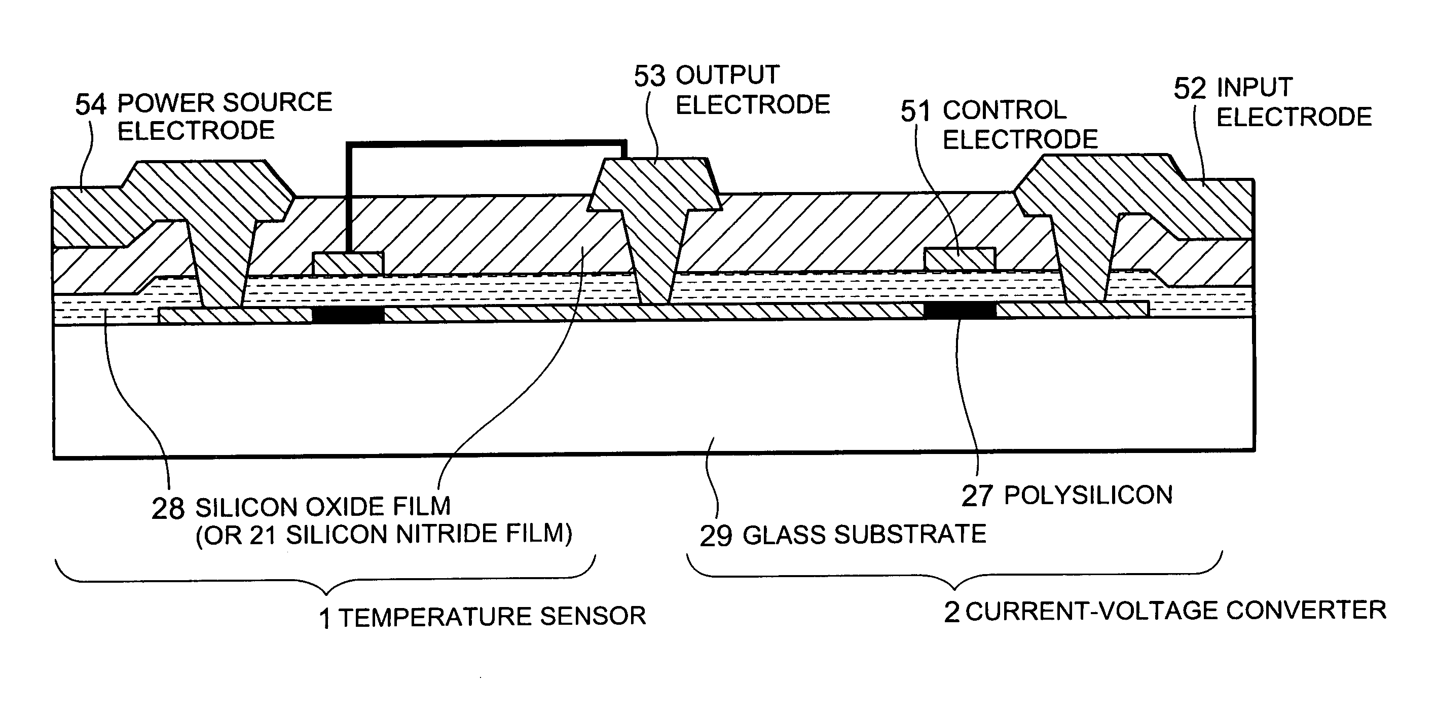
[0054]As shown in FIG. 4, this embodiment of the present invention has a fundamental feature of having a temperature sensor 1 and a current-voltage converter 2 on the same substrate. Current change due to temperature change of the substrate sensed by the temperature sensor 1 is converted to a voltage by the current-voltage converter 2. The temperature change of the substrate can be observed as voltage change.

[0055]FIG. 5A is a schematic diagram showing this. The temperature sensor 1 and the current-voltage converter 2 are each made of a thin-film transistor (TFT) and are formed on the pixel driving TFT array substrate. The gate electrode of the temperature sensor 1 is short-circuited with the source electrode and is connected to the drain electrode of the current-voltage converter 2. A constant negative dc voltage is applied to the power source electrode 54 of the temperature sensor 1. A constant input voltage is applied to the input electrode 52 of the current-...

second embodiment

[0074]This embodiment is different from the first embodiment in that the TFT is formed by the partially depleted SOI technology, not the polysilicon technology.

[0075]The SOI technology refers to a technology forming a single crystal silicon thin film on an insulator film formed on a substrate. The SOI technology is classified as the partially depleted SOI technology and the fully depleted SOI technology. The difference between both is the degree of depletion in a silicon film and specifically is divided based on the thickness of the silicon film. The process when the thickness of the silicon film is twice or more the thickness of the thickest depletion layer is called partially depleted SOI technology. The greatest thickness of the depletion layer depends on the amount of impurities and Fermi potential level and is different for each of the device technologies. The silicon film thicknesses of the partially depleted and the fully depleted are different for each of the device technolo...

third embodiment

[0085]This embodiment is different from First and Second Embodiments in that the TFT is formed by fully depleted SOI technology, not polysilicon technology. The fully depleted SOI technology is SOI technology wherein the thickness of the silicon film is less than the greatest thickness of the depletion layer. The thickness is generally 50 nm or less. The current-voltage converter adjusts the voltage applied to the gate electrode in the substrate direction (hereinafter, called a back gate voltage) by the fully depleted SOI technology so as to allow in a dummy manner the bottom part of the body region to be undepleted. The electrode applying the back gate voltage is called a back gate electrode. This structure can allow the back gate side of the depleted channel in the fully depleted SOI technology to be undepleted.

[0086]FIG. 23 shows an example the drain current-gate voltage dependence of the TFT manufactured by the fully depleted SOI technology. A drain current higher than that of t...


PUM


Abstract

A thin-film semiconductor device comprises a temperature sensor formed of a thin-film semiconductor and sensing a temperature as current, and a current-voltage converter formed of a thin-film semiconductor and having temperature dependence in which its current-voltage characteristic is different from that of the temperature sensor. A temperature sensed by the temperature sensor is converted to a voltage by the current-voltage converter.

Description

BACKGROUND OF THE INVENTION[0001]1. Field of the Invention[0002]The present invention relates to a thin-film semiconductor device, driving circuitry thereof, and an apparatus incorporating the same and using temperature information when operating them.[0003]2. Description of the Related Art[0004]Temperature sensors have been provided on the outside of display devices to permit temperature-dependent correction of the driving waveform for a liquid crystal display. Thermistors, platinum resistance thermometers, thermocouples, temperature sensors with a pn junction diode using bandgap, SAW (surface acoustic wave) temperature sensors, thermosensitive magnetic substances, and radiation thermometers using an infrared ray are mainly used. Temperature sensors with a pn junction diode, which is inexpensive and has a high linearity to temperature, are being widely used. An attempt to substitute light measurement of transmittance or reflectance for the temperature sensor is being made. A photod...

Claims


Application Information

Patent Timeline
Patent Type & Authority Patents(United States)
IPC IPC(8): H01L31/058
CPCG01K1/14G01K7/015G02F1/1362G01K2217/00Y10S257/93
Inventor TAKATORI, KENICHI
Owner HANNSTAR DISPLAY CORPORATION
Why Eureka
Try Eureka