Thin-film semiconductor device, circuitry thereof, and apparatus using them
a technology of thin film semiconductors and driving circuits, applied in the direction of instruments, heat measurement, electric/magnetic computing, etc., can solve the problems of easy to be noisy, and difficult to accurately measure a temperature when the liquid crystal is operated, etc., to achieve satisfactory image reproduction
- Summary
- Abstract
- Description
- Claims
- Application Information
AI Technical Summary
Benefits of technology
Problems solved by technology
Method used
Image
Examples
first embodiment
1 Basic Configuration
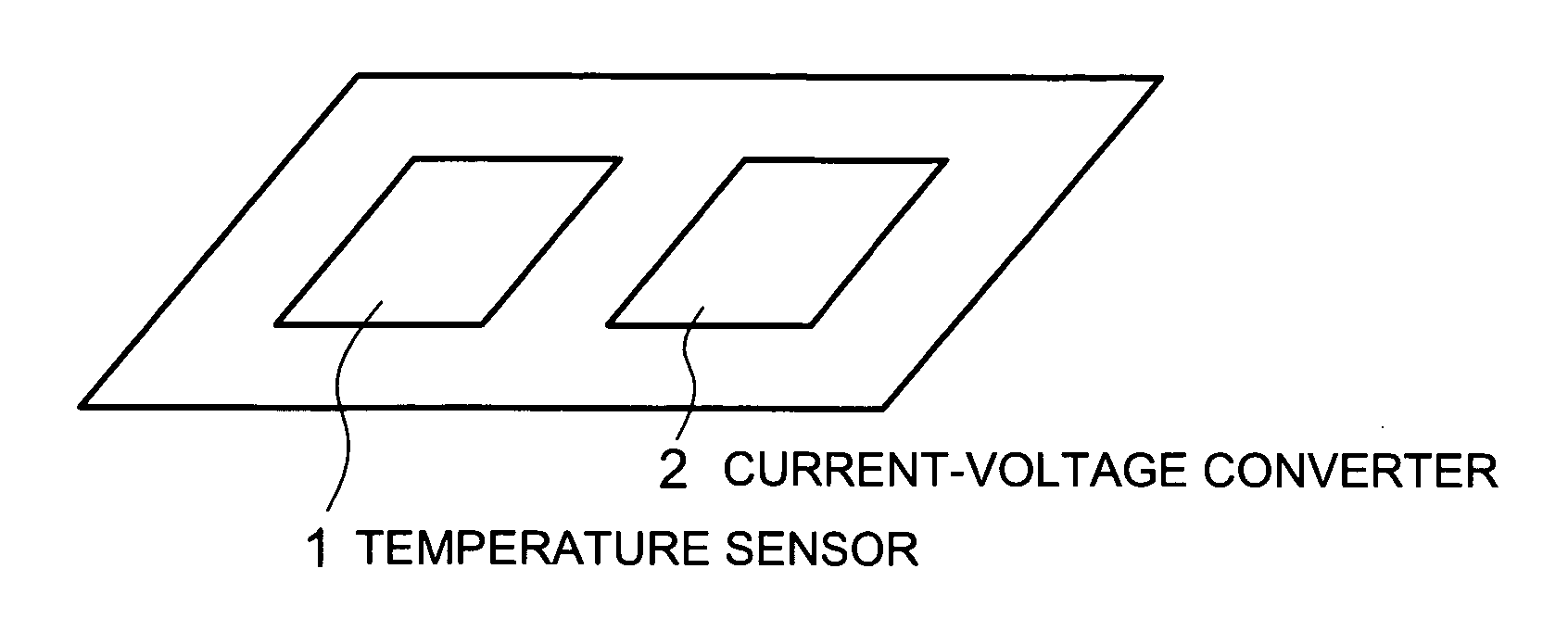
[0054] As shown in FIG. 4, this embodiment of the present invention has a fundamental feature of having a temperature sensor 1 and a current-voltage converter 2 on the same substrate. Current change due to temperature change of the substrate sensed by the temperature sensor 1 is converted to a voltage by the current-voltage converter 2. The temperature change of the substrate can be observed as voltage change.
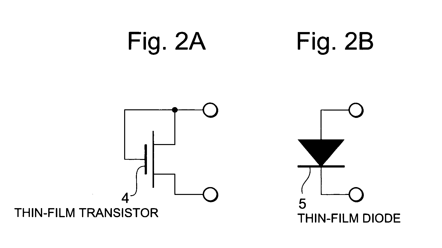
[0055]FIG. 5A is a schematic diagram showing this. The temperature sensor 1 and the current-voltage converter 2 are each made of a thin-film transistor (TFT) and are formed on the pixel driving TFT array substrate. The gate electrode of the temperature sensor 1 is short-circuited with the source electrode and is connected to the drain electrode of the current-voltage converter 2. A constant negative dc voltage is applied to the power source electrode 54 of the temperature sensor 1. A constant input voltage is applied to the input electrode 52 of the curr...
second embodiment
[0074] This embodiment is different from the first embodiment in that the TFT is formed by the partially depleted SOI technology, not the polysilicon technology.
[0075] The SOI technology refers to a technology forming a single crystal silicon thin film on an insulator film formed on a substrate. The SOI technology is classified as the partially depleted SOI technology and the fully depleted SOI technology. The difference between both is the degree of depletion in a silicon film and specifically is divided based on the thickness of the silicon film. The process when the thickness of the silicon film is twice or more the thickness of the thickest depletion layer is called partially depleted SOI technology. The greatest thickness of the depletion layer depends on the amount of impurities and Fermi potential level and is different for each of the device technologies. The silicon film thicknesses of the partially depleted and the fully depleted are different for each of the device techn...
third embodiment
[0085] This embodiment is different from First and Second Embodiments in that the TFT is formed by fully depleted SOI technology, not polysilicon technology. The fully depleted SOI technology is SOI technology wherein the thickness of the silicon film is less than the greatest thickness of the depletion layer. The thickness is generally 50 nm or less. The current-voltage converter adjusts the voltage applied to the gate electrode in the substrate direction (hereinafter, called a back gate voltage) by the fully depleted SOI technology so as to allow in a dummy manner the bottom part of the body region to be undepleted. The electrode applying the back gate voltage is called a back gate electrode. This structure can allow the back gate side of the depleted channel in the fully depleted SOI technology to be undepleted.
[0086]FIG. 23 shows an example the drain current-gate voltage dependence of the TFT manufactured by the fully depleted SOI technology. A drain current higher than that of...
PUM
 Abstract
Description
Claims
Application Information


